DS1923-F5#
Part Number : DS1923-F5#
Analog Devices Inc.The iButton® temperature/humidity logger (DS1923) is a rugged, self-sufficient system that measures temperature and/or humidity and records the result in a protected memory section. The recording is done at a user-defined rate. A total of 8192 8-bit readings or 4096 16-bit readings taken at equidistant intervals ranging from 1s to 273hrs can be stored. In addition to this, there are 512 bytes of SRAM for storing application-specific information and 64 bytes for calibration data. A mission to collect data can be programmed to begin immediately, or after a user-defined delay or after a temperature alarm. Access to the memory and control functions can be password-protected. The DS1923 is configured and communicates with a host-computing device through the serial 1-Wire® protocol, which requires only a single data lead and a ground return. Every DS1923 is factory-lasered with a guaranteed unique 64-bit registration number that allows for absolute traceability. The durable stainless-steel package is highly resistant to environmental hazards such as dirt, moisture, and shock. Accessories permit the DS1923 to be mounted on almost any object, including containers, pallets and bags.ApplicationsEnvironmental Studies/MonitoringTemperature and Humidity Logging in Food Preparation and ProcessingTransportation of Temperature- and Humidity-Sensitive Goods, Industrial ProductionWarehouse Monitoring
DS3231S#
Part Number : DS3231S#
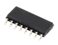
Analog Devices Inc.The DS3231 is a low-cost, extremely accurate I²C real-time clock (RTC) with an integrated temperature-compensated crystal oscillator (TCXO) and crystal. The device incorporates a battery input, and maintains accurate timekeeping when main power to the device is interrupted. The integration of the crystal resonator enhances the long-term accuracy of the device as well as reduces the piece-part count in a manufacturing line. The DS3231 is available in commercial and industrial temperature ranges, and is offered in a 16-pin, 300-mil SO package.The RTC maintains seconds, minutes, hours, day, date, month, and year information. The date at the end of the month is automatically adjusted for months with fewer than 31 days, including corrections for leap year. The clock operates in either the 24-hour or 12-hour format with an active-low AM/PM indicator. Two programmable time-of-day alarms and a programmable square-wave output are provided. Address and data are transferred serially through an I²C bidirectional bus.A precision temperature-compensated voltage reference and comparator circuit monitors the status of VCC to detect power failures, to provide a reset output, and to automatically switch to the backup supply when necessary. Additionally, the active-low RST pin is monitored as a pushbutton input for generating a µP reset.ApplicationsGlobal Positioning Systems (GPS)ServersTelematicsUtility Power Meters
EVAL-ADCMP563BRQZ
Part Number : EVAL-ADCMP563BRQZ
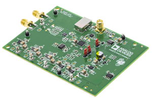
Analog Devices Inc.The ADCMP563/ADCMP564 are high speed comparatorsfabricated on Analog Devices’ proprietary XFCB process. Thedevices feature a 700 ps propagation delay with less than 75 psoverdrive dispersion. Dispersion, a measure of the difference inpropagation delay under differing overdrive conditions, is a particularlyimportant characteristic of high speed comparators. A separateprogrammable hysteresis pin is available on the ADCMP564.A differential input stage permits consistent propagation delaywith a wide variety of signals in the common-mode range from−2.0 V to +3.0 V. Outputs are complementary digital signals thatare fully compatible with ECL 10 K and 10 KH logic families.The outputs provide sufficient drive current to directly drivetransmission lines terminated in 50 Ω to −2 V. A latch input,which is included, permits tracking, track-and-hold, or sample-and-holdmodes of operation. The latch input pins contain internalpull-ups that set the latch in tracking mode when left open.The ADCMP563/ADCMP564 are specified over the industrialtemperature range (−40°C to +85°C).Applications Automatic test equipment High speed instrumentation Scope and logic analyzer front ends Window comparators High speed line receivers Threshold detection Peak detection High speed triggers Patient diagnostics Hand-held test instruments Zero crossing detectors Line receivers and signal restoration Clock drivers
LTC2626CDD-1#PBF
Part Number : LTC2626CDD-1#PBF
Analog Devices Inc.The LTC2606/LTC2616/LTC2626 are single 16-, 14- and 12-bit, 2.7V-to-5.5V rail-to-rail voltage output DACs in a 10-lead DFN package. They have built-in high performance output buffers and are guaranteed monotonic.These parts establish new board-density benchmarks for 16- and 14-bit DACs and advance performance standards for output drive and load regulation in single-supply, voltage-output DACs.The parts use a 2-wire, I2C compatible serial interface. The LTC2606/LTC2616/LTC2626 operate in both the standard mode (clock rate of 100kHz) and the fast mode (clock rate of 400kHz). An asynchronous DAC update pin (LDAC) is also included.The LTC2606/LTC2616/LTC2626 incorporate a power-on reset circuit. During power-up, the voltage outputs rise less than 10mV above zero scale; and after power-up, they stay at zero scale until a valid write and update take place. The power-on reset circuit resets the LTC2606-1/LTC2616-1/LTC2626-1 to midscale. The voltage outputs stay at midscale until a valid write and update take place.Applications Mobile Communications Process Control and Industrial Automation Instrumentation Automatic Test Equipment
MAX13080EASD+
Part Number : MAX13080EASD+
Analog Devices Inc.The MAX13080E–MAX13089E +5.0V, ±15kV ESD-protected, RS-485/RS-422 transceivers feature one driver and one receiver. These devices include fail-safe circuitry, guaranteeing a logic-high receiver output when receiver inputs are open or shorted. The receiver outputs a logic-high if all transmitters on a terminated bus are disabled (high impedance). The MAX13080E family include a hot-swap capability to eliminate false transitions on the bus during power-up or hot insertion.The MAX13080E/MAX13081E/MAX13082E feature reduced slew-rate drivers that minimize EMI and reduce reflections caused by improperly terminated cables, allowing error-free data transmission up to 250kbps. The MAX13083E/MAX13084E also feature slew-rate-limited drivers but allow transmit speeds up to 500kbps. The MAX13086E/MAX13087E/MAX13088E driver slew rates are not limited, making transmit speeds up to 16Mbps possible. The MAX13089E slew rate is pin selectable for 250kbps, 500kbps, and 16Mbps.The MAX13082E/MAX13088E are intended for half-duplex communications, and the MAX13080E/MAX13081E/MAX13083E/MAX13084E/MAX13086E/MAX13087E are intended for full-duplex communications. The MAX13089E is selectable for half-duplex or full-duplex operation. It also features independently programmable receiver and transmitter output phase through separate pins.The MAX13080E family transceivers draw 1.2mA of supply current when unloaded or when fully loaded with the drivers disabled. All devices have a 1/8-unit load receiver input impedance, allowing up to 256 transceivers on the bus.The MAX13080E/MAX13083E/MAX13086E/MAX13089E are available in 14-pin PDIP and 14-pin SO packages. The MAX13081E/MAX13082E/MAX13084E/MAX13087E/MAX13088E are available in 8-pin PDIP and 8-pin SO packages. The devices operate over the commercial, extended, and automotive temperature ranges.ApplicationsIndustrial ControlInstrumentationLighting SystemsPROFIBUSSecurity SystemsTelecomUtility Meters
MAX15013BASA+
Part Number : MAX15013BASA+
Analog Devices Inc.The MAX15012/MAX15013 high-frequency, 175V half-bridge, n-channel MOSFET drivers drive high- and low-side MOSFETs in high-voltage applications. These drivers are independently controlled and their 35ns typical propagation delay, from input to output, are matched to within 2ns (typ). The high-voltage operation with very low and matched propagation delay between drivers, and high source/sink current capabilities make these devices suitable for the high-power, high-frequency telecom power converters. A reliable on-chip bootstrap diode connected between VDD and BST eliminates the need for an external discrete diode.The MAX15012A/C and MAX15013A/C offer both noninverting drivers (see the Selector Guide of the full data sheet). The MAX15012B/D and MAX15013B/D offer a noninverting high-side driver and an inverting low-side driver. The MAX15012A/B/C/D feature CMOS (VDD/2) logic inputs. The MAX15013A/B/C/D feature TTL logic inputs. The drivers are available in the industry-standard 8-pin SO footprint and pin configuration and a thermally enhanced 8-pin SO package. All devices operate over the -40°C to +125°C automotive temperature range.ApplicationsActive-Clamp Forward ConvertersFull-Bridge ConvertersMotor ControlPower-Supply ModulesTelecom Half-Bridge Power SuppliesTwo-Switch Forward Converters
MAX15013BASA+T
Part Number : MAX15013BASA+T
Analog Devices Inc.The MAX15012/MAX15013 high-frequency, 175V half-bridge, n-channel MOSFET drivers drive high- and low-side MOSFETs in high-voltage applications. These drivers are independently controlled and their 35ns typical propagation delay, from input to output, are matched to within 2ns (typ). The high-voltage operation with very low and matched propagation delay between drivers, and high source/sink current capabilities make these devices suitable for the high-power, high-frequency telecom power converters. A reliable on-chip bootstrap diode connected between VDD and BST eliminates the need for an external discrete diode.The MAX15012A/C and MAX15013A/C offer both noninverting drivers (see the Selector Guide of the full data sheet). The MAX15012B/D and MAX15013B/D offer a noninverting high-side driver and an inverting low-side driver. The MAX15012A/B/C/D feature CMOS (VDD/2) logic inputs. The MAX15013A/B/C/D feature TTL logic inputs. The drivers are available in the industry-standard 8-pin SO footprint and pin configuration and a thermally enhanced 8-pin SO package. All devices operate over the -40°C to +125°C automotive temperature range.ApplicationsActive-Clamp Forward ConvertersFull-Bridge ConvertersMotor ControlPower-Supply ModulesTelecom Half-Bridge Power SuppliesTwo-Switch Forward Converters
MAX16002ATC+
Part Number : MAX16002ATC+
Analog Devices Inc.The MAX16000–MAX16007 are low-voltage, quad-/hex-/octal-voltage µP supervisors in small TQFN and TSSOP packages. These devices provide supervisory functions for complex multivoltage systems. The MAX16000/MAX16001/MAX16002 monitor four voltages, the MAX16003/MAX16004/MAX16005 monitor six voltages, and the MAX16006/MAX16007 monitor eight voltages. The MAX16000/MAX16001/MAX16003/MAX16004/MAX16006 offer independent outputs for each monitored voltage. The MAX16001/MAX16002/MAX16004–MAX16007 offer a reset output that asserts whenever any of the monitored voltages fall below their respective thresholds or the manual reset input is asserted. The reset output remains asserted for the reset timeout after all voltages are above their respective thresholds and the manual reset input is deasserted. The minimum reset timeout is internally set to 140ms or can be adjusted with an external capacitor.All open-drain outputs have internal 30µA pullups that eliminate the need for external pullup resistors. However, each output can be driven with an external voltage up to 5.5V. Other features offered include a manual reset input, a tolerance pin for selecting 5% or 10% input thresholds, and a margin enable function for deasserting the outputs during margin testing.The MAX16001/MAX16002/MAX16004–MAX16007 offer a watchdog timer that asserts active-low RESET or an independent watchdog output (MAX16005) when the watchdog timeout period (1.6s typ) is exceeded. The watchdog timer can be disabled by leaving the input open.These devices are offered in 12-, 16-, 20-, and 24-lead TQFN and 16-lead TSSOP packages. These are fully specified from -40°C to +125°C.ApplicationsMultivoltage ASICsNetworking/Telecommunication EquipmentServersStorage Equipment
MAX16029TG+
Part Number : MAX16029TG+
Analog Devices Inc.The MAX16025–MAX16030 are dual-/triple-/quad-voltagemonitors and sequencers that are offered in asmall TQFN package. These devices offer enormousdesign flexibility as they allow fixed and adjustablethresholds to be selected through logic inputs and providesequence timing through small external capacitors.These versatile devices are ideal for use in a widevariety of multivoltage applications.As the voltage at each monitored input exceeds itsrespective threshold, its corresponding output goeshigh after a propagation delay or a capacitor-set timedelay. When a voltage falls below its threshold, itsrespective output goes low after a propagation delay.Each detector circuit also includes its own enable input,allowing the power-good outputs to be shut off independently.The independent output for each detector isavailable with push-pull or open-drain configurationwith the open-drain version capable of supporting voltagesup to 28V, thereby allowing them to interface toshutdown and enable inputs of various DC-DC regulators.Each detector can operate independently as fourseparate supervisory circuits or can be daisy-chainedto provide controlled power-supply sequencing.The MAX16025–MAX16030 also include a reset functionthat deasserts only after all of the independentlymonitored voltages exceed their threshold. The resettimeout is internally fixed or can be adjusted externally.These devices are offered in a 4mm x 4mm TQFNpackage and are fully specified from -40°C to +125°C.ApplicationsDC-DC SuppliesMultivoltage SystemsNetworking/Telecommunication EquipmentServers/WorkstationsStorage Systems
MAX16803ATE+
Part Number : MAX16803ATE+
Analog Devices Inc.The MAX16803 current regulator operates from a 6.5V to 40V input-voltage range and delivers up to a total of 350mA to one or more strings of high-brightness LEDs (HB LEDs). The output current of the MAX16803 is adjusted by using an external current-sense resistor in series with the LEDs. A dimming input allows widerange 'pulsed' PWM operation. Wave-shaping circuitry reduces EMI. The differential current-sense input increases noise immunity. The MAX16803 is well suited for applications requiring high-voltage input and is able to withstand automotive load-dump events up to 40V. An on-board pass element minimizes external components while providing ±3.5% output-current accuracy. Additional features include a 5V regulated output and short-circuit and thermal protection.The MAX16803 is available in a thermally enhanced, 5mm x 5mm, 16-pin TQFN package and is specified over the automotive -40°C to +125°C temperature range.The MAX16836 is a newer and more cost effective product; except for different PWM dimming current slew rates, it provides the same performance and is pin-to-pin compatible with the MAX16803.ApplicationsAutomotive Exterior: Rear Combination Lights (RCL)Automotive Interior: Map, Courtesy, and Cluster LightingEmergency Vehicle Warning LightsGeneral LightingNavigation and Marine IndicatorsSignage, Gasoline Canopies, Beacons
MAX3643ETG+T
Part Number : MAX3643ETG+T
Analog Devices Inc.The MAX3643 burst-mode laser driver provides bias and modulation current drive for PON burst-mode ONT applications. It is specifically designed for use with a low-cost external controller for the APC (and if desired, AMC) loop. A high-speed differential burst-enable input enables the driver to switch the laser from a dark (output off) condition to full on condition in less than 2ns.When BEN is inactive, typical modulation and bias currents are 5µA each.Laser modulation current can be set from 10mA to 85mA and bias current can be set from 1mA to 70mA using the MODSET and BIASSET inputs. A sample-and-hold circuit is provided to capture the monitor diode output during short PON bursts, if needed, and the BEN high-speed signal is mirrored on an LVCMOS output to be used by the controller operating the APC/AMC loop.The MAX3643 burst-mode laser driver is packaged in a 4mm x 4mm, 24-pin thin QFN package. It operates from -40°C to +85°C.Applications1.25Gbps IEEE EPON ONT ModulesA/B/G/XGPON ONT Modules Up to 2.5Gbps
MAX4885ETJ+
Part Number : MAX4885ETJ+
Analog Devices Inc.The MAX4885 integrates high-bandwidth analog switches and level translating buffers to implement a complete 1:2 or 2:1 multiplexer for VGA signals. The device provides switching for RGB, display data channel (DDC), and horizontal and vertical synchronization (HSYNC, VSYNC) signals. A low-noise charge pump with internal capacitors provides a boosted gate-drive voltage to improve performance of the RGB switches. In the 1:2 multiplexer mode, HSYNC/VSYNC inputs feature level-shifting buffers to support low voltage CMOS or standard TTL-compatible graphics controllers. In the 2:1 multiplexer mode, the output buffers for the HSYNC/VSYNC inputs are disabled, allowing bidirectional signaling. In both modes, DDC signals are voltage-clamped to an external voltage to provide level translation and protection. The MAX4885 features a 5µA shutdown mode and is ESD protected to ±8kV human body model (HBM) on externally routed pins.The MAX4885 is specified over the extended (-40°C to +85°C) temperature range, and is available in the 32-pin, 5mm x 5mm TQFN package.ApplicationsNotebook ComputersServers
MAX5097BAUP+
Part Number : MAX5097BAUP+
Analog Devices Inc.The MAX5096/MAX5097 easy-to-use, Dual Mode™, DC-DC converters operate as LDO (low dropout) or switch-mode buck converters. At a high output load, the converters operate as high-efficiency pulse-width-modulated (PWM) switch-mode converters and reduce the power dissipation. The devices switch to a low-quiescent-current (IQ) LDO mode of operation at light load.During the key-off condition, the system's microcontroller drives the LDO/active-low BUCK input on the fly and forces the MAX5096/MAX5097 into LDO Mode, thereby reducing the quiescent current significantly.In Buck Mode, the MAX5096/MAX5097 operate from a 5V to 40V input voltage range and deliver up to 600mA of load current with excellent load and line regulation. The fixed-switching frequency versions of 135kHz and 330kHz are available. The MAX5096/MAX5097 DC-DC internal oscillator can be synchronized to an externalclock. External compensation and a current-mode control scheme make it easy to design with.In LDO Mode, the MAX5096/MAX5097 operate from a 4V to 40V input voltage. The LDO Mode operation is intended for a lower output load current of up to 100mA. The quiescent current at 100µA load in LDO Mode is only 41µA (typ).The MAX5096/MAX5097 feature an enable input that shuts down the device, reducing the current consumption to 6µA (typ). Additional features include a power-on reset output with a capacitor-adjustable timeout period, programmable soft-start, output tracking, output overload, short-circuit and thermal shutdown protections.The MAX5096/MAX5097 operate over the -40°C to +125°C automotive temperature range and are available in thermally enhanced 20-pin TSSOP or 16-pinTQFN packages.ApplicationsHome Security/Safety
MAX5128ELA+T
Part Number : MAX5128ELA+T
Analog Devices Inc.The MAX5128 nonvolatile, single, linear-taper, digitalpotentiometer performs the function of a mechanicalpotentiometer, but replaces the mechanics with a simple2-wire digital interface. The MAX5128 performs thesame function as a discrete potentiometer or variableresistor and features 128 taps and 22kΩ end-to-endresistance. The MAX5128 also features an ultra-small,2mm x 2mm µDFN package and low 0.5µA (typ) standbysupply current, making this device ideal for portableapplications. The MAX5128 operates from a +2.7V to+5.25V power supply. An integrated nonvolatile memoryrecalls the programmed wiper position of the digitalpotentiometer. A simple 2-wire up/down interface programsthe wiper position. The digital potentiometer providesa low 5ppm/°C ratiometric temperature coefficientand is specified over the extended -40°C to +85°C temperaturerange.ApplicationsBacklight AdjustmentBias Setting for RadiosFiber-Module Bias SettingLED Bias AdjustmentPortable Consumer ElectronicsPower-Supply ModulesVCOM Adjustment for LCD Panels
MAX5440EAG+
Part Number : MAX5440EAG+
Analog Devices Inc.The MAX5440 dual, 40kΩ logarithmic taper volume control features a debounced up/down interface for use with a simple rotary encoder without using a microcontroller (µC). Each potentiometer has 32 log-spaced tap points with a buffered wiper output and replaces mechanical potentiometers. An integrated bias generator provides the required ((VDD + VSS) / 2) bias voltage, eliminating the need for costly external op-amp circuits in unipolar audio applications. A mode-indicator LED output specifies volume or balance control. Five integrated LED drivers indicate volume level or balance settings, depending on the status of the mode indicator.The MAX5440 includes debounced pushbutton inputs for mute and mode. The mute input allows a single pushbutton to change between volume control and the -90dB (typ) mute setting. The mode input toggles between volume and balance control. A click-and-pop suppression feature minimizes the audible noise generated by wiper transitions. The MAX5440 provides a nominal temperature coefficient of 35ppm/°C end-to-end and 5ppm/°C, ratiometrically. The MAX5440 is available in a 24-pin SSOP package and is specified for operation over the -40°C to +85°C extended temperature range.ApplicationsDesktop SpeakersMultimedia Docking StationsSet-Top BoxesStereo Volume Control
MAX5954AETX+T
Part Number : MAX5954AETX+T
Analog Devices Inc.The MAX5954 hot-plug controller is designed for PCI Express® applications. The device provides hot-plug control for 12V, 3.3V, and 3.3V auxiliary supplies of a single PCI Express (PCI-E) slot. The MAX5954's logic inputs/outputs allow interfacing directly with the system hot-plug management controller or through an SMBus™ with an external I/O expander. Integrated debounced attention switch and present-detect signals are included to simplify system design.The MAX5954 drives two external n-channel MOSFETs to control the 12V and 3.3V main outputs. The 3.3V auxiliary output is controlled through an internal 0.3Ω n-channel MOSFET. An internal charge pump provides gate drive for the 12V output while the gate drive of the 3.3V output is driven by the 12V input supply. The 3.3V auxiliary output is completely independent from the main outputs with its own charge pump.At power-up, the MAX5954 keeps all of the external MOSFETs off until the supplies rise above their respective undervoltage lockout (UVLO) thresholds. The device keeps the internal MOSFET off only until the auxiliary input supply rises above its UVLO threshold. Upon a turn-on command, the MAX5954 enhances the external and internal MOSFETs slowly with a constant gate current to limit the power-supply inrush current. The MAX5954 actively limits the current of all outputs at all times and shuts down if an overcurrent condition persists for longer than a programmable overcurrent timeout. Thermal-protection circuitry also shuts down all outputs if the die temperature exceeds +150°C. After an overcurrent or overtemperature fault condition, the MAX5954L latches off while the MAX5954A automatically restarts after a restart time delay. The device is available in a 36-pin (6mm x 6mm) thin QFN package and operates over the -40°C to +85°C temperature range.ApplicationsDesktop/Mobile Server PlatformsEmbedded DevicesServersWorkstations
MAX6718AUKTID3+T
Part Number : MAX6718AUKTID3+T
Analog Devices Inc.The MAX6715A–MAX6729A/MAX6797A are ultra-low-voltage microprocessor (µP) supervisory circuits designed to monitor two or three system power-supply voltages. These devices assert a system reset if any monitored supply falls below its factory-trimmed or adjustable threshold and maintain reset for a minimum timeout period after all supplies rise above their thresholds. The integrated dual/triple supervisory circuits significantly improve system reliability and reduce size compared to separate ICs or discrete components.These devices monitor primary supply voltages (VCC1) from 1.8V to 5.0V and secondary supply voltages (VCC2) from 0.9V to 3.3V with factory-trimmed reset threshold voltage options (see the Reset Voltage Threshold Suffix Guide in the full data sheet). An externally adjustable RSTIN input option allows customers to monitor a third supply voltage down to 0.62V. These devices are guaranteed to be in the correct reset output logic state when either VCC1 or VCC2 remains greater than 0.8V.A variety of push-pull or open-drain reset outputs along with watchdog input, manual-reset input, and power-fail input/output features are available (see the Selector Guide in the full data sheet). Select reset timeout periods from 1.1ms to 1120ms (min) (see the Reset Timeout Period Suffix Guide in the full data sheet). The MAX6715A–MAX6729A/MAX6797A are available in small 5-, 6-, and 8-pin SOT23 packages and operate over the -40°C to +125°C temperature range.ApplicationsComputers/ServersIndustrial EquipmentMultivoltage SystemsPortable Battery-Powered EquipmentPrinters/Fax MachinesSet-Top BoxesTelecom/Networking Equipment
MAX6722AUTTGD2+T
Part Number : MAX6722AUTTGD2+T
Analog Devices Inc.The MAX6715A–MAX6729A/MAX6797A are ultra-low-voltage microprocessor (µP) supervisory circuits designed to monitor two or three system power-supply voltages. These devices assert a system reset if any monitored supply falls below its factory-trimmed or adjustable threshold and maintain reset for a minimum timeout period after all supplies rise above their thresholds. The integrated dual/triple supervisory circuits significantly improve system reliability and reduce size compared to separate ICs or discrete components.These devices monitor primary supply voltages (VCC1) from 1.8V to 5.0V and secondary supply voltages (VCC2) from 0.9V to 3.3V with factory-trimmed reset threshold voltage options (see the Reset Voltage Threshold Suffix Guide in the full data sheet). An externally adjustable RSTIN input option allows customers to monitor a third supply voltage down to 0.62V. These devices are guaranteed to be in the correct reset output logic state when either VCC1 or VCC2 remains greater than 0.8V.A variety of push-pull or open-drain reset outputs along with watchdog input, manual-reset input, and power-fail input/output features are available (see the Selector Guide in the full data sheet). Select reset timeout periods from 1.1ms to 1120ms (min) (see the Reset Timeout Period Suffix Guide in the full data sheet). The MAX6715A–MAX6729A/MAX6797A are available in small 5-, 6-, and 8-pin SOT23 packages and operate over the -40°C to +125°C temperature range.ApplicationsComputers/ServersIndustrial EquipmentMultivoltage SystemsPortable Battery-Powered EquipmentPrinters/Fax MachinesSet-Top BoxesTelecom/Networking Equipment
MAX6767TALD2+
Part Number : MAX6767TALD2+
Analog Devices Inc.The MAX6765–MAX6774B are low-quiescent-current, high-voltage linear regulators that operate from 4V to 72V and deliver up to 100mA of load current. These low-power devices consume only 31µA of quiescent current, making them ideal for always-on automotive modules. These devices are offered with fixed standard output options of 5.0V, 3.3V, 2.5V, and 1.8V, or can be adjusted from 1.8V to 11V with two external resistors.The MAX6765–MAX6774B feature a push-pull or open-drain, active-low RESET output with either fixed or adjustable thresholds. Whenever the regulator's output falls below the reset threshold, the active-low RESET output asserts and remains asserted for at least the minimum reset timeout period after the output voltage exceeds its threshold. The minimum reset timeout period is offered with fixed values from 75µs to 200ms or can be adjusted externally with a small capacitor.These devices provide three regulator enable modes to accommodate several power-on schemes. The MAX6765/MAX6766/MAX6769/MAX6770/MAX6773/MAX6773B/MAX6774 MAX6774B feature a single traditional enable input (ENABLE) to turn on and off the regulator. The MAX6771/MAX6772 provide dual enable inputs (ENABLE1 and ENABLE2) to turn on and off the regulator either through an ignition switch or a bus transceiver. The MAX6767/MAX6768 provide a hold input (active-low HOLD) in addition to the enable input to allow for the implementation of a self-holding circuit without requiring external components. Setting active-low HOLD low after enabling the regulator forces the regulator to remain on even if ENABLE is subsequently set low. Releasing active-low HOLD shuts down the regulator.The MAX6773/MAX6773B/MAX6774/MAX6774B also include a watchdog input that monitors a pulse train from the microprocessor (µP) and generates a reset pulse if the watchdog input remains high or low for a duration longer than the 1.6s (typ) (MAX6773/MAX6774) or 50ms (typ) (MAX6773B/MAX6774B) watchdog timeout period.The MAX6765–MAX6774B are available in a small, thermally enhanced 3mm x 3mm TDFN package that can dissipate up to 1.951W, thereby supporting continuous regulator operation during high ambient temperatures, high battery voltage, and high load-current conditions.The MAX6765–MAX6774B are fully specified for a -40°C to +125°C operating temperature range.ApplicationsAutomotiveIndustrialTelecom
MAX7319AEE+
Part Number : MAX7319AEE+
Analog Devices Inc.The MAX7319 2-wire serial-interfaced peripheral features eight input ports with selectable internal pullups, overvoltage protection to +6V, and transition detection with interrupt output.All input ports are continuously monitored for state changes (transition detection). Transitions are latched, allowing detection of transient changes. Any combination of inputs can be selected using the interrupt mask to assert the active-low INT output. When the MAX7319 is subsequently accessed through the serial interface, any pending interrupt is cleared.The +5.5V tolerant active-low RST input clears the serial interface, terminating any I²C communication to or from the MAX7319.The MAX7319 uses two address inputs with four-level logic to allow 16 I²C slave addresses. The slave address also enables or disables internal 40kΩ pullups in groups of four ports.The MAX7319 supports hot insertion. All eight input ports, the serial interface SDA, SCL, AD0, AD2, active-low INT, and active-low RST remain high impedance in power-down (V+ = 0) with up to +6V asserted on them.The MAX7319 is one device in a family of pin-compatible port expanders with a choice of input ports, open-drain I/O ports, and push-pull output ports.The MAX7319 is available in 16-pin QSOP and 16-pin TQFN packages, and is specified over the automotive temperature range (-40°C to +125°C).ApplicationsCell PhonesNotebooksSAN/NASSatellite RadioServers


