MAX44248EVKIT#
Part Number : MAX44248EVKIT#
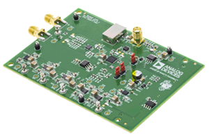
Analog Devices Inc.The MAX44244/MAX44245/MAX44248 family of parts provide ultra-precision, low-noise, zero-drift single/quad/ dual operational amplifiers featuring very low-power operation with a wide supply range. The devices incorporate a patented auto-zero circuit that constantly measures and compensates the input offset to eliminate drift over time and temperature as well as the effect of 1/f noise. These devices also feature integrated EMI filters to reduce high-frequency signal demodulation on the output. The op amps operate from either a single 2.7V to 36V supply or dual ±1.35V to ±18V supply. The devices are unity-gain stable with a 1MHz gain-bandwidth product and a low 90µA supply current per amplifier.The low offset and noise specifications and high supply range make the devices ideal for sensor interfaces and transmitters.The devices are available in µMAX®, SO, SOT23, and TSSOP packages and are specified over the -40°C to +125°C automotive operating temperature range.Applications4-20mA and 0 to 10V TransmittersPLC Analog I/O ModulesPortable Medical DevicesSensors InterfacesWeight Scales
MAX44250AUA+
Part Number : MAX44250AUA+
Analog Devices Inc.The MAX44250/MAX44251/MAX44252 are 20V, ultra-precision, low-noise, low-drift amplifiers that offer nearzero DC offset and drift through the use of patented auto-correlating zeroing techniques. This method constantly measures and compensates the input offset, eliminating drift over time and temperature and the effect of 1/f noise. These single, dual, and quad devices feature rail-to-rail outputs, operate from a single 2.7V to 20V supply or dual ±1.35V to ±10V supplies and consume only 1.15mA per channel, while providing 5.9nV/ input-referred voltage noise. The ICs are unity-gain stable with a gain-bandwidth product of 10MHz.With excellent specifications such as offset voltage of 6µV (max), drift of 19nV/°C (max), and 123nVP-P noise in 0.1Hz to 10Hz, the ICs are ideally suited for applications requiring ultra-low noise and DC precision such as interfacing with pressure sensors, strain gauges, precision weight scales, and medical instrumentation.The ICs are available in 5-pin SOT23, 8-pin SOT23, 8-pin µMAX®, and 14-pin SO packages and are rated over the -40°C to +125°C temperature range.ApplicationsLoad Cell and Bridge Transducer AmplificationMedical InstrumentationPrecision InstrumentationPressure TransducersStrain Gauges
MAX44269EWL+T
Part Number : MAX44269EWL+T
Analog Devices Inc.The MAX44269 is an ultra-small and low-power dual comparator ideal for battery-powered applications such as cell phones, notebooks, and portable medical devices that have extremely aggressive board space and power constraints. The comparator is available in a miniature 1.3mm x 1.3mm, 9-bump WLP package, making it the industry’s smallest dual comparator.The IC can be powered from supply rails as low as 1.8V and up to 5.5V. It requires just 0.5µA of typical supply current per comparator. It has a rail-to-rail input structure and a unique output stage that limits supply current surges while switching. This design also minimizes overall power consumption under dynamic conditions. The IC has open-drain outputs, making it suitable for mixed voltage systems. The IC also features internal filtering to provide high RF immunity. It operates over a -40°C to +85°C temperature range.ApplicationsBattery-Operated SensorsNotebooksPortable Medical Mobile AccessoriesSmartphonesTwo-Cell Battery-Powered DevicesUltra-Low-Power Systems
MAX44281OEVKIT#
Part Number : MAX44281OEVKIT#
Analog Devices Inc.The MAX44281 is the industry's first op amp in a 4-bump WLP package, designed for use in portable consumer and medical applications. This device is offered as a noninverting amplifier with gain (AV) of +1V/V, +2V/V, or +10V/V. The device features rail-to-rail output, low 100µV input voltage offset, and 15MHz of bandwidth with only 700µA of supply current. The device features shutdown functionality by pulling VDD to ground. During shutdown, both the input and the output are high impedance. The device is available in an ultra-small, 0.85mm x 0.85mm, 4-bump WLP package with 0.5mm height. It is specified over the -40°C to +125°C temperature range.Applications3G/4G HandsetsBattery-Powered DevicesGeneral-Purpose Signal ProcessingNotebooksPortable Medical DevicesSensor InterfacesTransimpedance Amplifiers
MAX4936ACTO+T
Part Number : MAX4936ACTO+T
Analog Devices Inc.The MAX4936A/MAX4937A are octal, high-voltage,transmit/receive (T/R) switches. The T/R switches arebased on a diode bridge topology, and the amount ofcurrent in the diode bridges can be programmed bythree digital inputs (S0, S1, and S2). Two control inputs(EN1 and EN2) allow enabling/disabling channels 1–4and channels 5–8, respectively. The MAX4936A includesthe T/R switch and grass-clipping diodes, performingboth transmit and receive operations. The MAX4937Aincludes just the T/R switch and performs the receiveoperation only.These devices feature low on-impedance in the entireultrasound frequency range with extremely low powerdissipation of 15mW (typ) per channel.The receive path for both devices is low impedanceduring low-voltage receive and high impedance duringhigh-voltage transmit, providing protection to the receivecircuitry. The low-voltage receive path is high bandwidth,low noise, low distortion, and low jitter.The MAX4936A SWC_ pins can be driven with high-voltagesignals using the anti-parallel diodes as grassclippers while connecting the SWB_ pins to the low-noiseamplifier (LNA). Connecting SWC_ to GND allowsthe internal anti-parallel diodes to be used as clamps.Grass-clipping diodes can then be connected to SWB_and the LNA to SWA_.Both devices are available in a small, 42-pin, 3.5mm x9mm TQFN package, and are specified over the commercial0°C to +70°C temperature range.ApplicationsHigh-Voltage Transmit and Low-Voltage IsolationMedical/Industrial ImagingUltrasound
MAX5217GUA+
Part Number : MAX5217GUA+
Analog Devices Inc.The MAX5215/MAX5217 are pin-compatible 14-bit and 16-bit digital-to-analog converters (DACs). TheMAX5215/MAX5217 are single-channel, low-powered, buffered voltage-output DACs. The devices use a precision external reference applied through the high resistance input for rail-to-rail operation and low system power consumption. The MAX5215/MAX5217 accept a wide 2.7V to 5.5V supply voltage range. Power consumption is extremely low to accommodate most low-power and low-voltage applications.The MAX5215/MAX5217 have an I²C-compatible, 2-wire serial interface that operates at clock rates up to 400kHz. On power-up, the MAX5215/MAX5217 reset the DAC output to zero, providing additional safety for applications that drive valves or other transducers that need to be off on power-up. The DAC output is buffered resulting in a low supply current of 80µA (max) and a low offset error of ±0.25mV. An asynchronous active-low input, AUX, is provided. This input can be programmed to support clear or load DAC operations, independent of the serial interface. The MAX5215/MAX5217 are available in an ultra-small (3mm x 5mm), 8-pin µMAX® package and are specified over the -40°C to +105°C extended industrial temperature range.ApplicationsAutomatic Test EquipmentAutomatic TuningCommunication SystemsData AcquisitionGain and Offset AdjustmentPortable InstrumentationPower Amplifier ControlProcess Control and Servo LoopsProgrammable Voltage and Current SourcesRemote Sensing
MAX5318GUG+T
Part Number : MAX5318GUG+T
Analog Devices Inc.The MAX5318 is a high-accuracy, 18-bit, serial SPI input, buffered voltage output digital-to-analog converter (DAC) in a 4.4mm x 7.8mm, 24-lead TSSOP package. The device features ±2 LSB INL (max) accuracy and a ±1 LSB DNL (max) accuracy over the full temperature range of -40°C to +105°C.The DAC voltage output is buffered resulting in a fast settling time of 3µs and a low offset and gain drift of ±0.5ppm/°C of FSR (typ). The force-sense output (OUT) maintains accuracy while driving loads with long lead lengths. Additionally, a separate AVSS supply, allows the output amplifier to go to 0V (GND) while maintaining full linearity performance.The MAX5318 includes user-programmable digital gain and offset correction to enable easy system calibration. At power-up, the device resets its outputs to zero or midscale. The wide 2.7V to 5.5V supply voltage range and integrated low-drift, low-noise reference buffer amplifier make for ease of use.The MAX5318 features a 50MHz, 3-wire, SPI interface. The MAX5318 is available in a 24-lead TSSOP package and operates over the -40°C to +105°C temperature range.ApplicationsAutomatic Test EquipmentAutomatic Tuning and CalibrationCommunication SystemsData-Acquisition SystemsGain and Offset AdjustmentMedical ImagingProcess Control and Servo LoopsProgrammable Voltage and Current SourcesTest and Measurement Equipment
MAX5805BAUB+T
Part Number : MAX5805BAUB+T
Analog Devices Inc.The MAX5803/MAX5804/MAX5805 single-channel, low-power, 8-/10-/12-bit, voltage-output digital-to-analog converters (DACs) include output buffers and an internal reference that is selectable to be 2.048V, 2.500V, or 4.096V. The MAX5803/MAX5804/MAX5805 accept a wide supply voltage range of 2.7V to 5.5V with extremely low power (< 1mW) consumption to accommodate most low-voltage applications. A precision external reference input allows rail-to-rail operation and presents a 100kΩ (typ) load to an external reference.The MAX5803/MAX5804/MAX5805 have an I2C-compatible, 2-wire interface that operates at clock rates up to 400kHz. The DAC output is buffered and has a low supply current of 155µA (typical at 3V) and a low offset error of ±0.5mV (typical). On power-up, the MAX5803/MAX5804/MAX5805 reset the DAC outputs to zero, providing additional safety for applications that drive valves or other transducers which need to be off on power-up. The internal reference is initially powered down to allow use of an external reference.The MAX5803/MAX5804/MAX5805 include a user-configurable active-low asynchronous input, active-low AUX for additional flexibility. This input can be programmed to asynchronously clear (active-low CLR) or temporarily gate (active-low GATE) the DAC output to a user-programmable value. A dedicated active-low asynchronous LDAC input is also included. This allows simultaneous output updates of multiple devices.The MAX5803/MAX5804/MAX5805 are available in 10-pin TDFN/µMAX® packages and are specified over the -40°C to +125°C temperature range.ApplicationsAutomatic Tuning and Optical ControlData AcquisitionGain and Offset AdjustmentPortable InstrumentationPower Amplifier Control and BiasingProcess Control and Servo LoopsProgrammable Voltage and Current Sources
MAX6070AAUT25+T
Part Number : MAX6070AAUT25+T
Analog Devices Inc.The MAX6070/MAX6071 offer a very low noise and low-drift voltage reference in a small 6-pin SOT23 package. These devices provide a 1/f noise voltage of only4.8µVP-P at an output voltage of 2.5V, with a temperature drift of 6ppm/°C (max, A grade). The devices consume 150µA of supply current and can sink and source up to 10mA of load current. The low-drift and low-noise specifications enable enhanced system accuracy, making these devices ideal for high-precision industrial applications. The MAX6070 offers a noise filter option for wideband applications.The devices are available in a 6-pin SOT23 package and specified over the extended industrial temperature range of -40°C to +125°C. The 2.5V options are alsoavailable in a 6-bump 0.78mm x 1.41mm wafer-level package (WLP).ApplicationsHigh-Accuracy Industrial and Process ControlHigh-Resolution ADCs and DACsPrecision Current SourcesPrecision Instrumentation
MAX6070BAUT12/V+T
Part Number : MAX6070BAUT12/V+T
Analog Devices Inc.The MAX6070/MAX6071 offer a very low noise and low-drift voltage reference in a small 6-pin SOT23 package. These devices provide a 1/f noise voltage of only4.8µVP-P at an output voltage of 2.5V, with a temperature drift of 6ppm/°C (max, A grade). The devices consume 150µA of supply current and can sink and source up to 10mA of load current. The low-drift and low-noise specifications enable enhanced system accuracy, making these devices ideal for high-precision industrial applications. The MAX6070 offers a noise filter option for wideband applications.The devices are available in a 6-pin SOT23 package and specified over the extended industrial temperature range of -40°C to +125°C. The 2.5V options are alsoavailable in a 6-bump 0.78mm x 1.41mm wafer-level package (WLP).ApplicationsHigh-Accuracy Industrial and Process ControlHigh-Resolution ADCs and DACsPrecision Current SourcesPrecision Instrumentation
MAX6071AAUT25+T
Part Number : MAX6071AAUT25+T
Analog Devices Inc.The MAX6070/MAX6071 offer a very low noise and low-drift voltage reference in a small 6-pin SOT23 package. These devices provide a 1/f noise voltage of only4.8µVP-P at an output voltage of 2.5V, with a temperature drift of 6ppm/°C (max, A grade). The devices consume 150µA of supply current and can sink and source up to 10mA of load current. The low-drift and low-noise specifications enable enhanced system accuracy, making these devices ideal for high-precision industrial applications. The MAX6070 offers a noise filter option for wideband applications.The devices are available in a 6-pin SOT23 package and specified over the extended industrial temperature range of -40°C to +125°C. The 2.5V options are alsoavailable in a 6-bump 0.78mm x 1.41mm wafer-level package (WLP).ApplicationsHigh-Accuracy Industrial and Process ControlHigh-Resolution ADCs and DACsPrecision Current SourcesPrecision Instrumentation
MAX9093AKA+T
Part Number : MAX9093AKA+T
Analog Devices Inc.The MAX9092/MAX9093/MAX9094/MAX9095 comparators are pin-for-pin compatible replacements for the LMX393/LMX393H/LMX339/LMX339H, respectively. The MAX9093/MAX9095 have the added benefit of internal hysteresis to provide noise immunity, preventing output oscillations even with slow-moving input signals.Advantages of the ICs include low supply voltage, small package, and low cost. They also offer a wide supply voltage range, wide operating temperature range, competitive CMRR and PSRR, response time characteristics, input offset, low noise, output saturation voltage, input bias current, and RF immunity.The ICs are available in both 8-pin SOT23/µMAX® and 14-pin TSSOP/SO packages.ApplicationsBattery-Powered ElectronicsGeneral-Purpose Low-Voltage ApplicationsGeneral-Purpose Portable DevicesMobile CommunicationsNotebooks and PDAs
MAX9273GTL+
Part Number : MAX9273GTL+
Analog Devices Inc.The MAX9273 compact serializer is designed to drive 50Ω coax or 100Ω shielded twisted-pair (STP) cable. The device pairs with the MAX9272 deserializer. The parallel input is programmable for single or double input. Double input allows higher pixel clock input frequency by registering two pixels of typical image-sensor video data before serializing. This doubles the maximum pixel clock frequency compared to single input. The device features an embedded control channel that operates at 9.6kbps to 1Mbps in UART and mixed UART/I²C modes, and up to 400kbps in I²C mode. Using the control channel, a microcontroller (µC) is capable of programming serializer, deserializer, and camera (or any peripheral) registers at any time, independent of video timing. There is one dedicated GPIO, four optional GPIOs, and a GPO output, allowing remote power-up of a camera module, camera frame synchronization, and other uses. Error-detection and correction coding are programmable. For driving longer cables, the serializer has programmable pre/deemphasis. Programmable spread spectrum is available on the serial output. The serial output meets ISO 10605 and IEC 61000-4-2 ESD standards. The core supply range is 1.7V to 1.9V and the I/O supply range is 1.7V to 3.6V. The device is available in a 40-pin (6mm × 6mm) TQFN-EP package with 0.5mm lead pitch and operates over the -40°C to +105°C temperature range.ApplicationsAutomotive Camera SystemsNavigation Displays
MAX9277GTM+
Part Number : MAX9277GTM+
Analog Devices Inc.The MAX9277/MAX9281 are 3.12Gbps Gigabit Multimedia Serial Link (GMSL) serializers with 3- or 4-data lane LVDS input (oLDI) and a CML serial output programmable for 50Ω coax or 100Ω shielded twisted pair (STP) cable drive. The MAX9281 has HDCP content protection but otherwise is the same as the MAX9277. The serializers pair with any GMSL deserializer capable of coax input. When programmed for STP output they are backward compatible with any GMSL deserializer. The output amplitude is programmable 100mV to 500mV single-ended (coax) or 100mV to 400mV differential (STP).The audio channel supports L-PCM I2S stereo and up to eight channels of L-PCM in TDM mode. Sample rates of 32kHz to 192kHz are supported with sample depth up to 32 bits.The embedded control channel operates at 9.6kbps to 1Mbps in UART-UART and UART-I2C modes, and up to 1Mbps in I2C-I2C mode. Using the control channel, a µC can program serializer, deserializer and peripheral device registers at any time, independent of video timing, and manage HDCP operation (MAX9281). A GPO output supports touch-screen controller interrupt requests from the remote end of the link.For use with longer cables, the serializers have programmable pre/deemphasis. Programmable spread spectrum is available on the serial output. The serial output meets ISO 10605 and IEC61000-4-2 ESD standards. The core supply is 1.7 to 1.9V and the I/O supply is 1.7 to 3.6V. The package is a lead-free, 48-pin, 7mm x 7mm TQFN with exposed pad and 0.5mm lead pitch.ApplicationsHigh-Resolution Automotive NavigationMegapixel Camera SystemsRear-Seat Infotainment
MAX9279GTN/V+
Part Number : MAX9279GTN/V+
Analog Devices Inc.The MAX9275/MAX9279 are 3.12Gbps Gigabit Multimedia Serial Link (GMSL) serializers with parallel LVCMOS inputs and a CML serial output programmable for 50Ω coax or 100Ω shielded twisted pair (STP) cable drive. The MAX9279 has HDCP content protection but otherwise is the same as the MAX9275. The serializers pair with any GMSL deserializer capable of coax input. When programmed for STP output they are backward compatible with any GMSL deserializer. The output amplitude is programmable 100mV to 500mV, single-ended (coax) or 100mV to 400mV differential (STP).The audio channel supports L-PCM I2S stereo and up to eight channels of L-PCM in TDM mode. Sample rates of 32kHz to 192kHz are supported with sample depth up to 32 bits.The embedded control channel operates at 9.6kbps to 1Mbps in UART-UART and UART-I2C modes, and up to 1Mbps in I2C-I2C mode. Using the control channel, a µC can program serializer, deserializer, and peripheral device registers at any time, independent of video timing, and manage HDCP operation (MAX9279). A GPO output supports touch-screen controller interrupt requests from the remote end of the link.For use with longer cables, the serializers have programmable pre/deemphasis. Programmable spread spectrum is available on the serial output. The serial output meets ISO10605 and IEC 61000-4-2 ESD standards. The core supply is 1.7 to 1.9V and the I/O supply is 1.7 to 3.6V. The MAX9275/MAX9279 are available in a lead-free, 56-pin, 8mm x 8mm, TQFN package with exposed pad and 0.5mm lead pitch.ApplicationsHigh-Resolution Automotive NavigationMegapixel Camera SystemsRear-Seat Infotainment
MAX98307ETE+
Part Number : MAX98307ETE+
Analog Devices Inc.The MAX98307/MAX98308 fully differential mono Class DG multilevel power amplifiers with integrated inverting charge pumps offer highly efficient, high-power audio solutions for portable applications.Class DG multilevel modulation extends the dynamic range of the output signal by employing a charge-pump-generated negative rail as needed to extend the supply voltage. This scheme results in high efficiency over a wide output power range.The ICs combine Maxim's active emissions limiting edge rate and overshoot control circuitry with multilevel output modulation to greatly reduce EMI. These features eliminate the need for output filtering as compared to traditional Class D devices, reducing component count and cost.The MAX98307's 16-pin TQFN package features an adjustable gain set by external resistors. The MAX98308's space-saving 12-bump WLP package features an internally fixed gain of 8.5dB, 11.5dB, 14.5dB, 17.5dB, and 20.5dB set by a single gain input. Both devices operate over the extended -40°C to +85°C temperature range.ApplicationsCellular PhonesNotebook ComputersPortable AudioSmartphonesTablet PCsVoIP Phones
ADUM3223CRZ
Part Number : ADUM3223CRZ
Analog Devices Inc.The ADuM3223/ADuM4223 are 4 A isolated, half-bridge gatedrivers that employ the Analog Devices, Inc., iCoupler® technology to provide independent and isolated high-side and low-sideoutputs. The ADuM3223 provides 3000 V rms isolation in thenarrow body, 16-lead SOIC package, and the ADuM4223 provides 5000 V rms isolation in the wide body, 16-lead SOIC package.Combining high speed CMOS and monolithic transformer technology, these isolation components provide outstanding performance characteristics superior to the alternatives, such as the combination of pulse transformers and gate drivers. The ADuM3223/ADuM4223 isolators each provide two independent isolated channels. They operate with an inputsupply ranging from 3.0 V to 5.5 V, providing compatibility with lower voltage systems. In comparison to gate drivers employinghigh voltage level translation methodologies, the ADuM3223/ADuM4223 offer the benefit of true, galvanic isolation between the input and each output. Each output may be continuously operated up to 537 V peak relative to the input, thereby supporting low-side switching to negative voltages. The differential voltagebetween the high-side and low-side may be as high as 800 V peak.As a result, the ADuM3223/ADuM4223 provide reliable controlover the switching characteristics of IGBT/MOSFET configurations over a wide range of positive or negative switching voltages.Applications Switching power supplies Isolated IGBT/MOSFET gate drives Industrial inverters Automotive
AD9146BCPZRL
Part Number : AD9146BCPZRL
Analog Devices Inc.The AD9146 is a dual, 16-bit, high dynamic range digital-to-analog converter (DAC) that provides a sample rate of 1230 MSPS, permitting multicarrier generation up to the Nyquist frequency.The AD9146 TxDAC+® includes features optimized for direct conversion transmit applications, including complex digital modulation, and gain and offset compensation. The DAC outputs are optimized to interface seamlessly with analog quadrature modulators, such as the ADL537x F-MOD series from Analog Devices, Inc. A 3-wire serial port interface provides for programming/readback of many internal parameters. Full-scale output current can be programmed over a range of 8.7 mA to 31.7 mA. The AD9146 comes in a 48-lead LFCSP.PRODUCT HIGHLIGHTS Ultralow noise and intermodulation distortion (IMD) enable high quality synthesis of wideband signals from baseband to high intermediate frequencies. A proprietary DAC output switching technique enhances dynamic performance. The current outputs are easily configured for various single-ended or differential circuit topologies. Compact LVDS digital interface offers reduced width data bus.APPILICATIONS Wireless infrastructure W-CDMA, CDMA2000, TD-SCDMA, WiMAX, GSM, LTE Digital high or low IF synthesis Transmit diversity Wideband communications: LMDS/MMDS, point-to-point
LTM2892CY-I#PBF
Part Number : LTM2892CY-I#PBF
Analog Devices Inc.The LTM2892 is a complete galvanic digital μModule® (micromodule) isolator. No external components are required. Individual 3V to 5.5V supplies power each side of the digital isolator. Separate logic supply pins allow easy interfacing with different logic levels from 1.62V to 5.5V, independent of the main supply.Module options are available with compatibility to SPI (LTM2892-S) and I2C (LTM2892-I), master mode only, specifications.Coupled inductors provide 3500VRMS of isolation between the input and output logic interface. This device is ideal for systems where the ground loop is broken, allowing uninterrupted communication through large common mode transients faster than 50kV/μs.Applications Isolated SPI or I2C Interfaces Industrial Systems Test and Measurement Equipment Breaking Ground Loops
LTM9010CY-14#PBF
Part Number : LTM9010CY-14#PBF
Analog Devices Inc.The LTM9011-14/LTM9010-14/LTM9009-14 are 8-channel, simultaneous sampling 14-bit A/D converters designed for digitizing high frequency, wide dynamic range signals. AC performance includes 73.1dB SNR and 88dB spurious free dynamic range (SFDR). Low power consumption per channel reduces heat in high channel count applications. Integrated bypass capacitance and flow-through pinout reduces overall board space requirements.DC specs include ±1LSB INL (typ), ±0.3LSB DNL (typ) and no missing codes over temperature. The transition noise is a low 1.2LSBRMS.The digital outputs are serial LVDS to minimize the number of data lines. Each channel outputs two bits at a time (2-lane mode). At lower sampling rates there is a one bit per channel option (1-lane mode).The ENC+ and ENC– inputs may be driven differentially or single-ended with a sine wave, PECL, LVDS, TTL, or CMOS inputs. An internal clock duty cycle stabilizer allows high performance at full speed for a wide range of clock duty cycles.Applications Communications Cellular Base Stations Software Defined Radios Portable Medical Imaging Multichannel Data Acquisition Nondestructive Testing


