
LTC6954IUFF-2#TRPBF
Part Number : LTC6954IUFF-2#TRPBF
Analog Devices Inc.The LTC6954 is a family of very low phase noise clock distribution parts. Each part has three outputs and each output has an individually programmable frequency divider and delay. There are four members of the family, differing in their output logic signal type:LTC6954-1: Three LVPECL outputsLTC6954-2: Two LVPECL and one LVDS/CMOS outputsLTC6954-3: One LVPECL and two LVDS/CMOS outputsLTC6954-4: Three LVDS/CMOS outputsEach output is individually programmable to divide the input frequency by any integer from 1 to 63, and to delay each output by 0 to 63 input clock cycles. The output duty cycle is always 50%, regardless of the divide number. The LVDS/CMOS outputs are jumper selectable via the OUTxSEL pins to provide either an LVDS logic output or a CMOS logic output.The LTC6954 also features Linear Technology’s EZSync system for perfect clock synchronization and alignment every time.All device settings are controlled through an SPI-compatible serial port.Applications Clocking High Speed, High Resolution ADCs, DACs and Data Acquisition Systems Low Jitter Clock Distribution
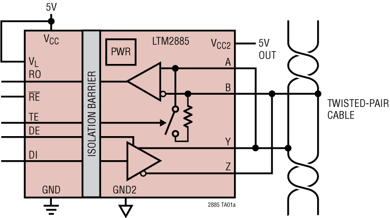
LTM2885CY#PBF
Part Number : LTM2885CY#PBF
Analog Devices Inc.The LTM2885 is a complete galvanically isolated full-duplex RS485/RS422 μModule® (micromodule) transceiver. No external components are required. A single supply powers both sides of the interface through an integrated, isolated, low noise, efficient 5V output DC/DC converter.Coupled inductors and an isolation power transformer provide 6500VRMS of isolation between the line transceiver and the logic interface. This device is ideal for systems where the ground loop is broken allowing for large common mode voltage variation. Uninterrupted communication is guaranteed for common mode transients up to 50kV/μs.Maximum data rates are 20Mbps or 250kbps in slew limited mode. Transmit data, DI, and receive data, RO, are implemented with event driven low jitter processing. The receiver has a one-eighth unit load supporting up to 256 nodes per bus. A logic supply pin allows easy interfacing with different logic levels from 1.62V to 5.5V, independent of the main supply.Enhanced ESD protection allows this part to withstand up to ±15kV (human body model) on the transceiver interface pins to isolated supplies and ±25kV through the isolation barrier to logic supplies without latch-up or damage.APPLICATIONS Isolated RS485/RS422 Interface Industrial Networks Breaking RS485 Ground Loops Isolated PROFIBUS-DP Networks
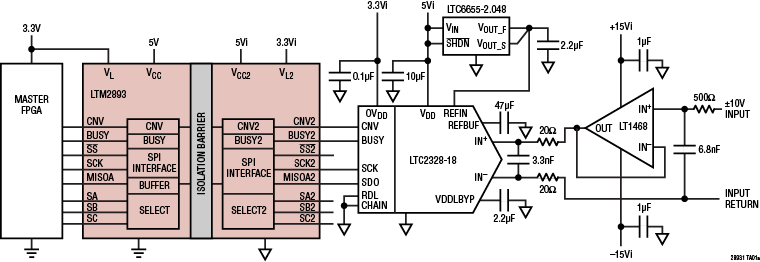
LTM2893IY#PBF
Part Number : LTM2893IY#PBF
Analog Devices Inc.The LTM2893 is a high speed isolated μModule (micromodule) SPI interface with ADC control signals. The LTM2893 is optimized for isolating 1Msps high resolution 18-bit SAR ADCs, such as the LTC2338 and similar families, and can interface with most general purpose ADCs. The LTM2893-1 is optimized for isolating the LTC2348 and similar families of simultaneous sampling ADCs that require writing configuration settings into the ADC. LTM2893 isolates the conversion start, sampling signal, with very low aperture jitter (30ps) and low latency (20ns).The interface enables fast throughput with no cycle latency, which makes the LTM2893 ideally suited for a wide variety of applications. The LTM2893 has a high speed SPI-compatible serial port that supports 1.71V to 5.5V logic and is configurable for ADCs with 8 to 32 bit SPI word lengths. It also isolates three select signals (SA, SB, SC) for controlling analog multiplexers or gain settings.The isolation barrier tolerates large voltage ground variations between the logic interface and the isolated side of the LTM2893. Uninterrupted communication is maintained during voltage transients greater than 50kV/μs.Applications Remote Sensing High Speed Data Acquisition Industrial Process Control Test and Measurement Equipment

LTM2894HY#PBF
Part Number : LTM2894HY#PBF
Analog Devices Inc.The LTM2894 is a complete galvanically-isolated USB 2.0 compatible μModule® (micromodule) transceiver.The LTM2894 is ideal for isolation in host, hub, bus splitter or peripheral device applications. It is compatible with USB 2.0 full speed (12Mbps) and low speed (1.5Mbps) operation. Automatic speed selection configures integrated pull-up resistors on the upstream port to match those sensed on the downstream device.The isolator μModule technology uses coupled inductors to provide 7500VRMS of isolation and 17.4mm of creepage between the upstream and downstream USB interface. This device is ideal for systems requiring isolated ground returns or large common mode voltage variations. Uninterrupted communication is guaranteed for common mode transients greater than 50kV/μs.Enhanced ESD protection allows this part to withstand up to ±20kV (human body model) on the USB transceiver interface pins to local supplies and ±20kV through the isolation barrier to supplies without latch-up or damage.Applications Isolated USB Interfaces Host, Hub, or Device Isolation Industrial/Medical Data Acquisition

LTM4639EY#PBF
Part Number : LTM4639EY#PBF
Analog Devices Inc.The LTM4639 is a complete 20A output high efficiency switch mode step-down DC/DC μModule (power module) regulator. Included in the package are the switching controller, power FETs, inductor and compensation components. Operating over an input voltage range from 2.375V to 7V, the LTM4639 supports an output voltage range of 0.6V to 5.5V, set by a single external resistor. Only a few input and output capacitors are needed.Current mode operation allows precision current sharing of up to four LTM4639 regulators to obtain up to 80A output. High switching frequency and a current mode architecture enable a very fast transient response to line and load changes without sacrificing stability. The device supports frequency synchronization, multiphase/current sharing, Burst Mode operation and output voltage tracking for supply rail sequencing. A diode-connected PNP transistor is included for use as an internal temperature monitor. For up to 20V input operation, please see the LTM4637.The LTM4639 is offered in a 15mm × 15mm × 4.92mm BGA package. The LTM4639 is RoHS compliant.Applications Telecom Servers and Networking Equipment Industrial Equipment Medical Systems High Ambient Temperature Systems 3.3V Input Systems

LTM4643MPY#PBF
Part Number : LTM4643MPY#PBF
Analog Devices Inc.The LTM4643 is a quad DC/DC step-down µModule (power module) regulator with 3A per output. Outputs can be paralleled in an array for up to 12A capability. Included in the package are the switching controllers, power FETs, inductors and support components. Operating over an input voltage range of 4V to 20V or 2.375V to 20V with an external bias supply, the LTM4643 supports an output voltage range of 0.6V to 3.3V each set by a single external resistor. Its high efficiency design delivers 3A continuous output current per channel. Only bulk input and output capacitors are needed.Fault protection features include overvoltage, overcurrent and overtemperature protection. The LTM4643 is offered in a 9mm ×15mm × 1.82mm LGA and 9mm × 15mm × 2.42mm BGA packages with SnPb (BGA) or RoHS compliant terminal finish.Applications FPGAs, GPUs and ASICs Applications PCIe and Backside PCB Mounting

MAX40200AUK+
Part Number : MAX40200AUK+
Analog Devices Inc.The MAX40200 is an ideal diode current-switch that drops so little voltage that it approaches an order of magnitude better than Schottky diodes.When forward-biased and enabled, the MAX40200 conducts with as little as 85mV of voltage drop while carrying currents as high as 1A. Typical voltage drop is 43mV at 500mA, with the voltage drop increasing linearly at higher currents. The MAX40200 thermally protects itself, and any downstream circuitry, from overtemperature conditions.When disabled (EN = low) the MAX40200 blocks voltages up to 6V in either direction, making it suitable for most low-voltage, portable electronic devices. The MAX40200 operates from a supply voltage of 1.5V to 5.5V.The MAX40200 is available in a tiny, 0.73mm X 0.73mm, 4-bump wafer-level package (WLP), with a 0.35mm bump pitch and only 0.5mm high and 5-pin SOT-23 package. The MAX40200 operates over the extended -40°C to +125°C temperature range.Design Solution: Cut Your Losses—With an Ideal Diode ›Design Solution: Design a Cooler, Safer Smart-Home Hub—Using an Ideal Diode ›How to Add a Diode ORing or Battery Backup Circuit Using the MAX40200 Ideal DiodeApplicationsCellular PhonesElectronic ToysNotebook and Tablet ComputersPortable Media PlayersPortable/Wearable Medical DevicesUSB-Powered Peripherals

MAX44286TAZS+T
Part Number : MAX44286TAZS+T
Analog Devices Inc.The MAX44286 is a zero-drift, high-side current-sense amplifier family that offers precision, low supply current and is available in a tiny 4-bump ultra-thin WLP of 0.78mm x 0.78mm x 0.35mm footprint. This miniature size is of paramount for today’s applications in smartphones, mobile accessories, notebooks, portable medical, and all battery-operated portable devices where current monitoring with precision and space are critical. The MAX44286 has voltage output offered in four gain versions of 25V/V, 50V/V, 100V/V, and 200V/V. These four gain versions offer flexibility in the choice of the sense resistor and the very low input offset voltage helps in detecting small currents on the orders of low microamps. Low power capability also offers the possibility of minimizing power dissipation.The MAX44286 operates with a supply voltage range of 1.6V to 5.5V over the -40°C to +85°C temperature range and from 1.8V to 5.5V over the -40°C to +125°C automotive temperature range. Supply voltage for the device is shared with the RS+ pin to fit the MAX44286 in a 4-bump, ultra-thin WLP package.ApplicationsMobile AccessoriesNotebook Computers and TabletsPortable MedicalPortable/Battery-Powered SystemsPower Management SystemsSmartphones
LTC1149CS-5#PBF
Part Number : LTC1149CS-5#PBF
Analog Devices Inc.Switching Voltage Regulators Hi Eff Sync Buck Sw Regs
LTC3630AMPDHC#PBF
Part Number : LTC3630AMPDHC#PBF
Analog Devices Inc.Switching Voltage Regulators Hi Eff, 76V 500mA Sync Buck Conv

LTC4236CUFD-1#PBF
Part Number : LTC4236CUFD-1#PBF
Analog Devices Inc.Hot Swap Voltage Controllers 2x Ideal Diode-OR & 1x Hot Swap Cntr w/

DS4560S-AR+
Part Number : DS4560S-AR+
Analog Devices Inc.The DS4560 is a self-contained hot-plug switch intended to be used on +12V power buses to limit through current and to control the power-up output-voltage ramp. The device contains an on-board 25mΩ n-channel power MOSFET that is actively closed-loop controlled to ensure that an adjustable current limit is not exceeded. The maximum allowable current through the device is determined by an external resistor connected to the ILIM pin.The DS4560 also contains the ability to control the power-up output-voltage ramp. A capacitor connected to the VRAMP pin sets the desired voltage ramp rate. The output voltage is unconditionally clamped to keep input overvoltage stresses from harming the load. The DS4560 also contains an adjustable power-up timer. A capacitor connected to the TIMER pin determines how long after power-on reset the DS4560 should wait before starting to apply power to the load. The TIMER pin can also be driven with a digital logic output to create a device-enable function.The DS4560 contains an on-board temperature sensor with hysteresis. If operating conditions cause the device to exceed an internal thermal limit, the DS4560 either unconditionally shuts down and latches off awaiting a power-on reset (DS4560S-LO), or it waits until the device has cooled by the hysteresis amount and then restarts (DS4560S-AR).ApplicationsBase StationsInfiniBand™PCI/PCI Express®RAID/Hard DrivesServers/Routers

LTC2216CUP#PBF
Part Number : LTC2216CUP#PBF
Analog Devices Inc.The LTC2216/LTC2215 are 80Msps/65Msps sampling 16- bit A/D converters designed for digitizing high frequency, wide dynamic range signals with input frequencies up to 400MHz. The input range of the ADC is fixed at 2.75VP-P.The LTC2216/LTC2215 are perfect for demanding communications applications, with AC performance that includes 81.5dBFS noise floor and 100dB spurious free dynamic range (SFDR). Ultra low jitter of 85fsRMS allows undersampling of high input frequencies while maintaining excellent noise performance. Maximum DC specs include ±3.5LSB INL, ±1LSB DNL (no missing codes). The digital output can be either differential LVDS or single-ended CMOS. There are two format options for the CMOS outputs: a single bus running at the full data rate or demultiplexed buses running at half data rate. A separate output power supply allows the CMOS output swing to range from 0.5V to 3.6V. The ENC+ and ENC– inputs may be driven differentially or single-ended with a sine wave, PECL, LVDS, TTL or CMOS inputs. An optional clock duty cycle stabilizer allows high performance at full speed with a wide range of clock duty cycles.Applications Telecommunications Receivers Cellular Base Stations Spectrum Analysis Imaging Systems ATE

LTC2636CMS-LZ8#PBF
Part Number : LTC2636CMS-LZ8#PBF
Analog Devices Inc.The LTC2636 is a family of octal 12-, 10-, and 8-bit voltage-output DACs with an integrated, high-accuracy, low-drift 10ppm/°C reference in 14-lead DFN and 16-lead MSOP packages. It has a rail-to-rail output buffer and is guaranteed monotonic. The LTC2636-L has a full-scale output of 2.5V, and operates from a single 2.7V to 5.5V supply. The LTC2636-H has a full-scale output of 4.096V, and operates from a 4.5V to 5.5V supply. Each DAC can also operate with an external reference, which sets the DAC full-scale output to the external reference voltage.These DACs communicate via an SPI/MICROWIRE-compatible 3-wire serial interface which operates at clock rates up to 50MHz. Hardware clear (CLR) and asynchronous DAC update (LDAC) pins are available in the MSOP package. The LTC2636 incorporates a power-on reset circuit. Options are available for reset to zero-scale or reset to mid-scale in internal reference mode, or reset to mid-scale in external reference mode after power-up.Applications Mobile Communications Process Control and Industrial Automation Automatic Test Equipment Portable Equipment Automotive Optical Networking
LTC2636HMS-LMI12#PBF
Part Number : LTC2636HMS-LMI12#PBF
Analog Devices Inc.The LTC2636 is a family of octal 12-, 10-, and 8-bit voltage-output DACs with an integrated, high-accuracy, low-drift 10ppm/°C reference in 14-lead DFN and 16-lead MSOP packages. It has a rail-to-rail output buffer and is guaranteed monotonic. The LTC2636-L has a full-scale output of 2.5V, and operates from a single 2.7V to 5.5V supply. The LTC2636-H has a full-scale output of 4.096V, and operates from a 4.5V to 5.5V supply. Each DAC can also operate with an external reference, which sets the DAC full-scale output to the external reference voltage.These DACs communicate via an SPI/MICROWIRE-compatible 3-wire serial interface which operates at clock rates up to 50MHz. Hardware clear (CLR) and asynchronous DAC update (LDAC) pins are available in the MSOP package. The LTC2636 incorporates a power-on reset circuit. Options are available for reset to zero-scale or reset to mid-scale in internal reference mode, or reset to mid-scale in external reference mode after power-up.Applications Mobile Communications Process Control and Industrial Automation Automatic Test Equipment Portable Equipment Automotive Optical Networking
LTC2636HMS-LZ10#PBF
Part Number : LTC2636HMS-LZ10#PBF
Analog Devices Inc.The LTC2636 is a family of octal 12-, 10-, and 8-bit voltage-output DACs with an integrated, high-accuracy, low-drift 10ppm/°C reference in 14-lead DFN and 16-lead MSOP packages. It has a rail-to-rail output buffer and is guaranteed monotonic. The LTC2636-L has a full-scale output of 2.5V, and operates from a single 2.7V to 5.5V supply. The LTC2636-H has a full-scale output of 4.096V, and operates from a 4.5V to 5.5V supply. Each DAC can also operate with an external reference, which sets the DAC full-scale output to the external reference voltage.These DACs communicate via an SPI/MICROWIRE-compatible 3-wire serial interface which operates at clock rates up to 50MHz. Hardware clear (CLR) and asynchronous DAC update (LDAC) pins are available in the MSOP package. The LTC2636 incorporates a power-on reset circuit. Options are available for reset to zero-scale or reset to mid-scale in internal reference mode, or reset to mid-scale in external reference mode after power-up.Applications Mobile Communications Process Control and Industrial Automation Automatic Test Equipment Portable Equipment Automotive Optical Networking
LTC2636IDE-HMI10#PBF
Part Number : LTC2636IDE-HMI10#PBF
Analog Devices Inc.The LTC2636 is a family of octal 12-, 10-, and 8-bit voltage-output DACs with an integrated, high-accuracy, low-drift 10ppm/°C reference in 14-lead DFN and 16-lead MSOP packages. It has a rail-to-rail output buffer and is guaranteed monotonic. The LTC2636-L has a full-scale output of 2.5V, and operates from a single 2.7V to 5.5V supply. The LTC2636-H has a full-scale output of 4.096V, and operates from a 4.5V to 5.5V supply. Each DAC can also operate with an external reference, which sets the DAC full-scale output to the external reference voltage.These DACs communicate via an SPI/MICROWIRE-compatible 3-wire serial interface which operates at clock rates up to 50MHz. Hardware clear (CLR) and asynchronous DAC update (LDAC) pins are available in the MSOP package. The LTC2636 incorporates a power-on reset circuit. Options are available for reset to zero-scale or reset to mid-scale in internal reference mode, or reset to mid-scale in external reference mode after power-up.Applications Mobile Communications Process Control and Industrial Automation Automatic Test Equipment Portable Equipment Automotive Optical Networking
LTC2636IDE-HMI12#PBF
Part Number : LTC2636IDE-HMI12#PBF
Analog Devices Inc.The LTC2636 is a family of octal 12-, 10-, and 8-bit voltage-output DACs with an integrated, high-accuracy, low-drift 10ppm/°C reference in 14-lead DFN and 16-lead MSOP packages. It has a rail-to-rail output buffer and is guaranteed monotonic. The LTC2636-L has a full-scale output of 2.5V, and operates from a single 2.7V to 5.5V supply. The LTC2636-H has a full-scale output of 4.096V, and operates from a 4.5V to 5.5V supply. Each DAC can also operate with an external reference, which sets the DAC full-scale output to the external reference voltage.These DACs communicate via an SPI/MICROWIRE-compatible 3-wire serial interface which operates at clock rates up to 50MHz. Hardware clear (CLR) and asynchronous DAC update (LDAC) pins are available in the MSOP package. The LTC2636 incorporates a power-on reset circuit. Options are available for reset to zero-scale or reset to mid-scale in internal reference mode, or reset to mid-scale in external reference mode after power-up.Applications Mobile Communications Process Control and Industrial Automation Automatic Test Equipment Portable Equipment Automotive Optical Networking
LTC2636IDE-HMX8#PBF
Part Number : LTC2636IDE-HMX8#PBF
Analog Devices Inc.The LTC2636 is a family of octal 12-, 10-, and 8-bit voltage-output DACs with an integrated, high-accuracy, low-drift 10ppm/°C reference in 14-lead DFN and 16-lead MSOP packages. It has a rail-to-rail output buffer and is guaranteed monotonic. The LTC2636-L has a full-scale output of 2.5V, and operates from a single 2.7V to 5.5V supply. The LTC2636-H has a full-scale output of 4.096V, and operates from a 4.5V to 5.5V supply. Each DAC can also operate with an external reference, which sets the DAC full-scale output to the external reference voltage.These DACs communicate via an SPI/MICROWIRE-compatible 3-wire serial interface which operates at clock rates up to 50MHz. Hardware clear (CLR) and asynchronous DAC update (LDAC) pins are available in the MSOP package. The LTC2636 incorporates a power-on reset circuit. Options are available for reset to zero-scale or reset to mid-scale in internal reference mode, or reset to mid-scale in external reference mode after power-up.Applications Mobile Communications Process Control and Industrial Automation Automatic Test Equipment Portable Equipment Automotive Optical Networking
LTC2636IDE-HMX8#TRPBF
Part Number : LTC2636IDE-HMX8#TRPBF
Analog Devices Inc.The LTC2636 is a family of octal 12-, 10-, and 8-bit voltage-output DACs with an integrated, high-accuracy, low-drift 10ppm/°C reference in 14-lead DFN and 16-lead MSOP packages. It has a rail-to-rail output buffer and is guaranteed monotonic. The LTC2636-L has a full-scale output of 2.5V, and operates from a single 2.7V to 5.5V supply. The LTC2636-H has a full-scale output of 4.096V, and operates from a 4.5V to 5.5V supply. Each DAC can also operate with an external reference, which sets the DAC full-scale output to the external reference voltage.These DACs communicate via an SPI/MICROWIRE-compatible 3-wire serial interface which operates at clock rates up to 50MHz. Hardware clear (CLR) and asynchronous DAC update (LDAC) pins are available in the MSOP package. The LTC2636 incorporates a power-on reset circuit. Options are available for reset to zero-scale or reset to mid-scale in internal reference mode, or reset to mid-scale in external reference mode after power-up.Applications Mobile Communications Process Control and Industrial Automation Automatic Test Equipment Portable Equipment Automotive Optical Networking


