MAX20019ATBA/V+T
Part Number : MAX20019ATBA/V+T
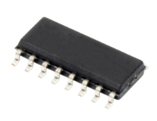
Analog Devices Inc.MAX20019/MAX20020 are 2.2MHz and 3.2MHz dual step-down converters with integrated high-side and low-side MOSFETs. The high-voltage step-down converter is designed for continuous operation up to 17V input voltages. The output voltage is factory preset. Buck 1 is preset to 3.3V, 3.0V, or 2.8V. Buck 2 is preset to 1.8V, 1.5V, 1.2V, or 1V. Another option is Buck 1 preset to 5V and Buck 2 preset to 3.3V. The low-voltage buck features fixed-frequency PWM- mode operation with a switching frequency of 2.2MHz or 3.2MHz. High-frequency operation allows for an all-ceramic capacitor design and small-size external components. The low-resistance on-chip switches ensure high efficiency while minimizing critical inductance. A 500mV enable hysteresis on the MAX20019 allows the use of long, low-cost coax cables, even during slow startup situations. The MAX20020’s Buck 1 starts after VSUP is greater than 5.5V and Buck 1 is driven by the EN input. Protection features include overvoltage (OV) protection, cycle-by-cycle current limit, and thermal shutdown with automatic recovery. The buck converters operate 180° out-of-phase from each other to minimize input-current ripple. Design Solution: Provide a Safe Power Path from the Car Battery toRemote Cameras ›Design Solution: How to Miniaturize Your Automotive Remote Camera ›ApplicationsAutomotive Point-of-LoadSurround-View Camera Power Supplies
MAX20019ATBB/V+T
Part Number : MAX20019ATBB/V+T
Analog Devices Inc.MAX20019/MAX20020 are 2.2MHz and 3.2MHz dual step-down converters with integrated high-side and low-side MOSFETs. The high-voltage step-down converter is designed for continuous operation up to 17V input voltages. The output voltage is factory preset. Buck 1 is preset to 3.3V, 3.0V, or 2.8V. Buck 2 is preset to 1.8V, 1.5V, 1.2V, or 1V. Another option is Buck 1 preset to 5V and Buck 2 preset to 3.3V. The low-voltage buck features fixed-frequency PWM- mode operation with a switching frequency of 2.2MHz or 3.2MHz. High-frequency operation allows for an all-ceramic capacitor design and small-size external components. The low-resistance on-chip switches ensure high efficiency while minimizing critical inductance. A 500mV enable hysteresis on the MAX20019 allows the use of long, low-cost coax cables, even during slow startup situations. The MAX20020’s Buck 1 starts after VSUP is greater than 5.5V and Buck 1 is driven by the EN input. Protection features include overvoltage (OV) protection, cycle-by-cycle current limit, and thermal shutdown with automatic recovery. The buck converters operate 180° out-of-phase from each other to minimize input-current ripple. Design Solution: Provide a Safe Power Path from the Car Battery toRemote Cameras ›Design Solution: How to Miniaturize Your Automotive Remote Camera ›ApplicationsAutomotive Point-of-LoadSurround-View Camera Power Supplies
MAX20047AFPA/V+
Part Number : MAX20047AFPA/V+
Analog Devices Inc.The MAX20047 is an automotive-grade, low-cost, small-footprint dual-port charger IC designed for automotive charging applications. It combines a fully synchronous 6A step-down buck converter with integrated high-side and low-side FETs capable of operating with input voltages from 3.5V to 36V and delivering 5.2V output voltage. The IC features integrated iPod®/iPhone®1.0A and iPad® 2.1A dedicated charging modes.The IC delivers up to 3A of charging current with 93% efficiency per port through integrated switches with programmable current limit and thermal foldback control. The buck converter switching frequency is programmable from 0.4MHz to 2.2MHz. Short-to-ground protection and overcurrent protection are also provided on the protected HVBUS outputs to protect the internal BUS power rail from an overcurrent fault. The MAX20047 offers short-to-battery up to +18V and can also be ordered with spread-spectrum operation to reduce EMI. iPod, iPhone, and iPad are registered trademarks of Apple Inc.. Design Solution: Beat the Heat: Build a Compact, Multi-StandardDual USB Charger ›ApplicationsAutomotive Cigarette Lighter AdaptersPower Supply for Linear ChargersUSB Dedicated Charging Ports (DCP)
MAX20077ATCE/VY+T
Part Number : MAX20077ATCE/VY+T
Analog Devices Inc.The MAX20077/MAX25277 is a small, synchronous buck converter with integrated high-side and low-side switches. The device is designed to deliver up to 2.5A (2.0A for the MAX20077ATCC/VY+ variant) with 3.5V to 36V input voltages while using only 3.5μA quiescent current at no load.The device provides an accurate output voltage of ±2% in FPWM mode within the normal 6V to 18V operation input range. With 20ns minimum on-time capability, the converter is capable of large input-to-output conversion ratios. Voltage quality can be monitored by observing the PGOOD signal. The device can operate in dropout by running at 99% duty cycle, making it ideal for automotive and industrial applications. The device offers two fixed 5V and 3.3V output voltages. In addition, the device can be configured for 1V to 10V output voltages using an external resistor-divider. Frequency is internally fixed at 2.1MHz, which allows for small external components and reduced output ripple, and guarantees no AM interference. A 400kHz option is also offered to provide minimum switching losses and maximum efficiency. The device automatically enters skip mode at light loads with ultra-low 3.5μA quiescent current at no load. The device offers pin-enabled spread-spectrum frequency modulation designed to minimize EMI-radiated emissions due to the modulation frequency.The MAX20077/MAX25277 variants are available in a small (3mm x 3mm), 12-pin, side-wettable TDFN package with an exposed pad, and require very few external components.ApplicationsAutomotiveHigh-Voltage DC-DC ConvertersIndustrial
MAX20084BATEA/VY+
Part Number : MAX20084BATEA/VY+
Analog Devices Inc.The MAX20084B is a dual-antenna power supply with an I2C interface for diagnostics and control. The dual 270mA antenna supplies are linear regulators whose output voltage is set individually through I2C. Additionally, internal registers are used to set the current limit, open-load threshold, and other parameters.An internal 8-bit ADC allows the channel current to be measured. The AOUT analog output can also be used with an external ADC to measure the output current on either channel.The MAX20084B is available in two variants: the MAX20084BATEA/VY+ with both channels turned off by default after power-up, and the MAX20084BATEB/VY+ with channel 1 turned on by default after power-up.The MAX20084B is available in a 4mm x 4mm, side-wettable TQFN package and operates over the -40°C to +125°C temperature range.ApplicationsAutomotive Camera and Sensor PowerAutomotive Microphone PowerRemote LNA Phantom Power
MAX20086ATPA/VY+T
Part Number : MAX20086ATPA/VY+T
Analog Devices Inc.The MAX20086–MAX20089 dual/quad camera power protector ICs deliver up to 600mA load current to each of their four output channels. Each output is individually protected from short-to-battery, short-to-ground, and overcurrent conditions. The ICs operate from a 3V to 5.5V supply and with a 3V to 15V camera supply. The input-to-output voltage drop is only 110mV (typ) at 300mA. The ICs provide an enable input and I2C interface to read the diagnostic status of the device. An on-board ADC enables reading of the current through each switch. The ASIL B- and ASIL D-compliant versions include support for reading an additional seven diagnostic measurements through the ADC, ensuring high-fault coverage. The MAX20086–MAX20089 include overtemperature shutdown and overcurrent limiting on each output channel separately. All devices are designed to operate from -40°C to +125°C ambient temperature. Design Solution: Provide a Safe Power Path from the Car Battery toRemote Cameras ›ApplicationsPower-over-Coax for Radar and Camera ModulesSurround-View Camera ECU
MAX20087ATPB/VY+
Part Number : MAX20087ATPB/VY+
Analog Devices Inc.The MAX20086–MAX20089 dual/quad camera power protector ICs deliver up to 600mA load current to each of their four output channels. Each output is individually protected from short-to-battery, short-to-ground, and overcurrent conditions. The ICs operate from a 3V to 5.5V supply and with a 3V to 15V camera supply. The input-to-output voltage drop is only 110mV (typ) at 300mA. The ICs provide an enable input and I2C interface to read the diagnostic status of the device. An on-board ADC enables reading of the current through each switch. The ASIL B- and ASIL D-compliant versions include support for reading an additional seven diagnostic measurements through the ADC, ensuring high-fault coverage. The MAX20086–MAX20089 include overtemperature shutdown and overcurrent limiting on each output channel separately. All devices are designed to operate from -40°C to +125°C ambient temperature. Design Solution: Provide a Safe Power Path from the Car Battery toRemote Cameras ›ApplicationsPower-over-Coax for Radar and Camera ModulesSurround-View Camera ECU
MAX20088ATPA/VY+
Part Number : MAX20088ATPA/VY+
Analog Devices Inc.The MAX20086–MAX20089 dual/quad camera power protector ICs deliver up to 600mA load current to each of their four output channels. Each output is individually protected from short-to-battery, short-to-ground, and overcurrent conditions. The ICs operate from a 3V to 5.5V supply and with a 3V to 15V camera supply. The input-to-output voltage drop is only 110mV (typ) at 300mA. The ICs provide an enable input and I2C interface to read the diagnostic status of the device. An on-board ADC enables reading of the current through each switch. The ASIL B- and ASIL D-compliant versions include support for reading an additional seven diagnostic measurements through the ADC, ensuring high-fault coverage. The MAX20086–MAX20089 include overtemperature shutdown and overcurrent limiting on each output channel separately. All devices are designed to operate from -40°C to +125°C ambient temperature. Design Solution: Provide a Safe Power Path from the Car Battery toRemote Cameras ›ApplicationsPower-over-Coax for Radar and Camera ModulesSurround-View Camera ECU
MAX20331EWL+T
Part Number : MAX20331EWL+T
Analog Devices Inc.The MAX20331/MAX20331A are overvoltage ICs designed to protect the audio codecs and electronics of portable devices. Connecting the MAX20331/MAX20331A between the 3.5mm jack and audio path electronics provides protection against high-voltage conditions to ±40V.The MAX20331/MAX20331A are available in a space-saving, 9-bump, 0.4mm pitch, 1.23mm x 1.23mm wafer-level package (WLP) and operate over the -40°C to +85°C extended temperature range.ApplicationsSmart PhonesTablets
MAX20335BEWX+T
Part Number : MAX20335BEWX+T
Analog Devices Inc.The MAX20335 is a battery-charge-management solution ideal for low-power wearable applications. The device includes a linear battery charger with a smart power selector and several power-optimized peripherals. The MAX20335 features two ultra-low quiescent current buck regulators and three ultra-low quiescent current low-dropout (LDO) linear regulators, providing up to five regulated voltages, each with an ultra-low quiescent current, allows designers to minimize power consumption and extend battery life in 24/7 operation devices, such as those in the wearable market.The battery charger features a smart power selector that allows operation on a dead battery when connected to a power source. To avoid overloading a power adapter, the input current to the smart power selector is limited based on an I2C register setting. If the charger power source is unable to supply the entire system load, the smart power control circuit supplements the system load with current from the battery. The charger also supports temperature dependent charge currents.The two synchronous, high-efficiency step-down buck regulators feature a variable frequency mode for increased efficiency during light-load operation. The output voltage of these regulators can be programmed through I2C with the default preconfigured. The buck regulators cansupport dynamic voltage scaling to further improve system power consumption.The three configurable LDOs each have a dedicated input pin. Each LDO regulator output voltage can be programmed through I2C with the default preconfigured. The linear regulators can also be configured to operate as power switches that may be used to disconnect the quiescent load of the system peripherals.The MAX20335 features a programmable power controller that allows the device to be configured for applications that require the device be in a true-off, or always-on, state. The controller also provides a delayed reset signal and voltage sequencing.The MAX20335 is available in a 36-bump, 0.4mm pitch, 2.72mm x 2.47mm wafer-level package (WLP).ApplicationsFitness MonitorsRechargeable IoT devicesWearable Electronics
MAX20355EWO+
Part Number : MAX20355EWO+
Analog Devices Inc.The MAX20355 is a Power Line Communication (PLC) master with ModelGaugeTM m5 EZ fuel gauge and buckboost converter. The MAX20355 and MAX20357 provide a complete system solution for charging and data transfer between a charging case and a battery-powered device over a single contact.The PLC interface is capable of 100kpbs throughput while simultaneously providing 400mA of total charging/system current. A 4Mbaud half-duplex dataonly UART mode provides an easy and fast method forfirmware updates, debugging interface, and factory modes.MAX20355 utilizes a 3.3W buck-boost converter with dynamic voltage scaling (DVS) to automatically manage the charging voltage based on the slave device MAX20357 control signal.Additional features include comprehensive slave device insertion and removal notifications, moisture detection, overcurrent protection, and 8kV contact rated ESD protection on the PLC outputs.APPLICATIONS TWS Headphones Augmented Reality Glasses Wearable Devices
AD4684BCPZ-RL
Part Number : AD4684BCPZ-RL
Analog Devices Inc.The AD4684/AD4685 are 16-bit, dual, simultaneous sampling, high speed, successive approximation register (SAR), analog-to-digital converters (ADCs) that operate from a 3.0 V to 3.6 V power supply and feature throughput rates of up to 1 MSPS for the AD4684 and 500 kSPS for the AD4685. The analog input types are single-ended and are sampled and converted on the falling edge of CS.The AD4684/AD4685 have an on-chip sequencer and integrated on-chip oversampling block to improve dynamic range and reduce noise at lower bandwidths. A buffered internal 2.5 V reference is included. Alternatively, an external reference up to 3.3 V can be used. The conversion process and data acquisition use standard control inputs, allowing interfacing to microprocessors or digital signal processors (DSPs). The AD4684/AD4685 is compatible with 1.8 V, 2.5 V, and 3.3 V interfaces by using the separate logic supply. The AD4684/AD4685 are available in a 16-lead, 3 mm × 3 mm lead frame chip scale package (LFCSP) with operation specified from −40°C to +125°C.PRODUCT HIGHLIGHTS 4-channel, dual simultaneous sampling ADC. Pin-compatible product family. High throughput rate: 1 MSPS (AD4684) and 500 kSPS (AD4685). Space-saving, 16-lead, 3 mm × 3 mm LFCSP. Integrated oversampling block to increase dynamic range and SNR and to reduce SCLK speed requirements. Single-ended analog inputs. Small sampling capacitor reduces amplifier drive burden. APPLICATIONS Motor control position feedback Motor control current sense Sonars Power quality Data acquisition systems Erbium doped fiber amplifier (EDFA) applications Inphase and quadrature demodulation
ADA4945-1ACPZ-R7
Part Number : ADA4945-1ACPZ-R7
Analog Devices Inc.The ADA4945-1 is a low noise, low distortion, fully differential amplifier with two selectable power modes. The device operates over a broad power supply range of 3 V to 10 V. The low dc offset, dc offset drift, and excellent dynamic performance of the ADA4945-1 makes it well suited for a variety of data acquisition and signal processing applications. The device is an ideal choice for driving high resolution, high performance successive approximation register (SAR) and Σ-Δ analog-to-digital converters (ADCs) on 4 mA of quiescent current (full power mode). The device can also be selected to operate on 1.4 mA of quiescent current (low power mode) to scale the power consumption to the desired performance necessary for an ADC drive application. The adjustable common-mode voltage allows the ADA4945-1 to match the input common-mode voltage of multiple ADCs. The internal common-mode feedback loop provides exceptional output balance, as well as suppression of even order harmonic distortion products.With the ADA4945-1, differential gain configurations are achieved with a simple external feedback network of four resistors determining the closed-loop gain of the amplifier. The ADA4945-1 is fabricated using Analog Devices, Inc., proprietary, silicon germanium (SiGe), complementary bipolar process, enabling the device to achieve low levels of distortion with an input voltage noise of only 1.8 nV/√Hz (full power mode).The ADA4945-1 is available in a RoHS-complaint, 3 mm × 3 mm, 16-lead LFCSP. The ADA4945-1 is specified to operate from −40°C to +125°C.Applications Low power Σ-Δ, PulSAR®, and SAR ADC drivers Single-ended to differential converters Differential buffers Medical imaging Process control Portable electronics
ADBMS2952WCCSZ
Part Number : ADBMS2952WCCSZ
Analog Devices Inc.ADBMS2950 and ADBMS2952 are Battery Pack Monitors for electrical and hybrid vehicles, and other current or voltage sense applications. ADBMS2950 and ADBMS2952 measure the current flowing in and out of a battery pack by sensing the voltage drop over a shunt resistor with a very low offset.ADBMS2950 and ADBMS2952 also detect Overcurrent conditions using fast Overcurrent ADCs with digital threshold comparators and communicate their results through dedicated Overcurrent alert lines with minimum delay.ADBMS2950 and ADBMS2952 feature a total of 12 internally buffered high impedance inputs for measuring voltages from external sensors or resistor dividers, enabling measurement of pack voltages, temperatures, HV-Link voltages, chassis isolation, and the supervision of the state of contactors and fuses. Six digital outputs (GPO) supporting open-drain or push-pull can be used to control high voltage transistors to disconnect external resistor dividers. Four digital general-purpose inputs/outputs (GPIO) also allow operation as an I2C or SPI controller interface to address an external EEPROM or other serial peripherals.The built-in serial interface of ADBMS2950 can be configured for SPI or isolated isoSPI communication to the host. An additional isoSPI port allows to connect a daisy chain of ADBMS2950 devices; optionally extended with ADBMS6830 or ADBMS6832 (ADBMS683x) Cell Monitors. The ADBMS2952 supports SPI communication only.APPLICATIONS Electric and Hybrid Electric Vehicles Backup Battery Systems Grid Energy Storage
LTC9101AUF-2#PBF
Part Number : LTC9101AUF-2#PBF
Analog Devices Inc.The LTC9101-2 chipset is a 12/24-port power sourcing equipment (PSE) controller designed for use in IEEE 802.3bt Type 3 and 4 compliant Power over Ethernet (PoE) systems. The LTC9101-2/LTC9102 is designed to power compliant 802.3af, 802.3at, and 802.3bt PDs. The LTC9101-2/LTC9102 chipset delivers lowest-in-industry heat dissipation by utilizing low RDS(ON) external MOSFETs and 0.1Ω sense resistance per power channel. A transformer-isolated communication protocol replaces expensive opto-couplers and complex isolated 3.3V supply, resulting in significant BOM cost savings.Advanced power management features include per-port 14‑bit current/voltage monitoring, programmable power limits, and versatile fast shut down of preselected ports. An advanced power management host software layer is available. PD detection uses a proprietary multipoint detection mechanism ensuring excellent immunity from false PD identification. Autoclass and 5-event physical classification are supported. The LTC9101-2/LTC9102 includes an I2C serial interface operable up to 1MHz. The LTC9101-2/LTC9102 is pin or I2C programmable to negotiate PD delivered power up to 71.3W.APPLICATIONS PoE PSE Switches/Routers and Midspans
LTC9101AUF-3#PBF
Part Number : LTC9101AUF-3#PBF
Analog Devices Inc.The LTC9101-3/LTC9103 chipset is a 8/16-port power sourcing equipment (PSE) controller and power manager designed for use in IEEE 802.3at compliant Power over Ethernet (PoE) systems. The LTC9101-3 manages a user-defined system-level power budget across all ports. Port power is automatically assigned based on system power availability, initial physical classification and after power up, port dynamic power consumption.The LTC9101-3 prioritizes port power by port number (port 1 is highest priority) and automatically removes power from lower priority ports to accommodate higher priority ports.The LTC9101-3 features an interface to control an external serial LED driver. LED indications include Port On, Port Off, Port Power Denied, and Port Fault states. A Supply Overload LED indicates system power usage is near power limit or a port is being denied power.The LTC9101-3 operates without a host present. Configuration is accomplished by pin settings and I2C-based flash programming.The LTC9101-3 autonomously performs compliant 802.3at detection, classification power up, power on, and fault management.APPLICATIONS Small Business PoE PSE Switches/Routers
LTM8080MPY#PBF
Part Number : LTM8080MPY#PBF
Analog Devices Inc.The LTM8080 is a 40VIN, dual 500mA or single 1A ultralow noise, ultrahigh PSRR μModule® regulator. LTM8080 has cascaded architecture which contains a 40VIN step-down Silent Switcher regulator with an integrated EMI noise shield followed by dual high-performance low dropout linear regulators. The dual LDOs feature ADI’s ultralow noise and ultrahigh PSRR architecture for powering noise-sensitive applications. The LTM8080 is an integrated solution comprised of a switcher and LDOs, which offers both advantages while maintaining a small size and significantly reduced PCB layout sensitivity.The package includes the controllers, power switches, inductors, and support components. In addition, the LTM8080 has a built-in voltage tracking function that automatically sets VBUS to either 2.5V nominal or 1V higher than VOUT1, whichever is greater, to achieve superior noise performance and minimize power dissipation.The LTM8080 is packaged in a thermally enhanced, compact (9mm × 6.25mm × 3.32mm) over-molded Ball Grid Array (BGA) package suitable for automated assembly by standard surface mount equipment and is RoHS compliant.APPLICATIONS RF Power Supplies: PLLs, VCOs, Mixers, LNAs Very Low Noise Instrumentation High Speed/High Precision Data Converters Medical Applications: Imaging, Diagnostics
MAX22192ARC+T
Part Number : MAX22192ARC+T
Analog Devices Inc.The MAX22192 is an IEC 61131-2 compliant industrialdigital input device with integrated digital isolation. TheMAX22192 translates eight, 24V current-sinking, industrialinputs to an isolated serialized SPI-compatible outputthat interfaces with 1.71V to 5.5V logic voltage. A current-settingresistor allows the MAX22192 to be configured forType 1, Type 2, or Type 3 inputs. For proximity switches,the field-wiring is verified using the wire break feature.When wire break is enabled, the active-low LFAULT output is assertedand a register flag set if the input current drops belowthe wire break threshold for more than 20ms. Additionaldiagnostics that assert active-low LFAULT include: overtemperatureprotection, low 24V field supply, 24V field supply missing,and CRC communication error.For robust operation in industrial environments, each inputincludes a programmable glitch filter. The filter delay oneach channel can be independently programmed to oneof eight values between 50µs and 20ms, or filter bypass.The MAX22192 has an isolated 4-pin SPI interface, andin addition uses isolated active-low LLATCH input for synchronizinginput data across multiple devices in parallel, and isolatedactive-low LFAULT output for instantly alerting the host of anydiagnostic issues. The digital signals with a name startingwith L are logic-side signals, and the digital signals with aname starting with F are field-side signals.The MAX22192 field-side accepts a single 7V to 65V supplyto the VDD24F pin. When powered by the field supply,the MAX22192 generates a 3.3V output on the VDD3F pinfrom an integrated LDO regulator, which can provide up to25mA of current for external loads in addition to poweringthe MAX22192. Alternatively, the MAX22192 can be poweredfrom a 3.0V to 5.5V supply connected to the VDD3Fpin. The logic-side of the MAX22192 is powered from asingle 1.71V to 5.5V supply to the VDDL pin to interfacewith 1.8V, 3.3V, or 5V logic levels.The MAX22192 has an isolation rating of 600VRMS for 60seconds and is available in a 70-pin GQFN package with2.3mm clearance and creepage. The package materialhas a minimum comparative tracking index (CTI) of 600V,which gives it a group I rating in creepage tables.ApplicationsIndustrial AutomationProcess AutomationProgrammable Logic Controllers
MAX22513ATI+
Part Number : MAX22513ATI+
Analog Devices Inc.The MAX22513 dual-channel low power IO-Link device transceiver features a selectable control interface, internal high-efficiency DC-DC buck regulator, two internal linear regulators, and integrated surge protection for robust communication. The device features low-on resistance drivers (C/Q and DO/DI), selectable driver current limits, and overcurrent protection to reduce power dissipation in small sensor applications.The DC-DC buck regulator supplies up to 300mA load current and has an adjustable output voltage (from 2.5V to 12V). Internal linear regulators generate 5V and 3.3V, supplying up to 50mA of current. The MAX22513 can be controlled using SPI or I2C interfaces, providing flexibility for microcontrollers, and extensive control and diagnostic features. Both full- and half-duplex SPI are supported. The internal MCLK oscillator provides a clock source to a microcontroller for IO-Link communication.The MAX22513 features extensive integrated protection to ensure robust communication in harsh industrial environments. All four IO pins (V24, C/Q, DO/DI, and GND), are reverse voltage protected, short circuit protected, and feature integrated ±1kV/500Ω surge protection.The MAX22513 is available in a tiny WLP package (4.1mm x 2.1mm) or 28-pin TQFN-EP package (3.5mm x 5.5mm) and operates over the -40°C to +125°C temperature range.ApplicationsIndustrial SensorsIO-Link Sensor and Actuator Devices
MAX25201ATEC/VY+T
Part Number : MAX25201ATEC/VY+T
Analog Devices Inc.The MAX25201/MAX25202 are high-performance, current-mode PWM controllers with 1.5μA (typ) shutdown current for wide input voltage range boost converters. The 4.5V to 36V input operating voltage range makes these devices ideal in automotive applications, such as front-end preboost or general-purpose boost power supply, for the first boost stage in high-power LED lighting applications or to generate audio amplifier voltages. An internal low-dropout regulator with a 5V output voltage enables the MAX25201/MAX25202 to operate directly from an automotive battery input. The input operating range can be extended to as low as 1.8V after startup.The MAX25201/MAX25202’s switching frequency operation (up to 2.2MHz) reduces output ripple, avoids AM band interference, and allows for the use of smaller external components. The switching frequency is resistor adjustable from 220kHz to 2.2MHz. Alternatively, the frequency can be synchronized to an external clock. A spread- spectrum option is available to improve system EMI performance. For high-current applications the dual-phase MAX25202 is available. The MAX25202 operates at a fixed 400kHz switching frequency and can be synchronized to an external clock.The controllers feature a power-OK monitor and undervoltage lockout. Protection features include cycle-by-cycle current limit and thermal shutdown. The MAX25201/MAX25202 operate over the -40°C to +125°C automotive temperature range.ApplicationsCluster SystemsE-callInfotainment Systems


