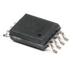
AD680ARZ-REEL7
Part Number : AD680ARZ-REEL7
Analog Devices Inc.VOLT REF, SOIC-8, 2.5V, -40 TO 85DEG C;
ADR5045BRTZ-REEL7
Part Number : ADR5045BRTZ-REEL7
Analog Devices Inc.VOLT REF, 5V, SOT-23-3, -40 TO 125DEG C;

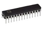
LT1021CCN8-5#PBF
Part Number : LT1021CCN8-5#PBF
Analog Devices Inc.VOLT REF, DIP-8, 5V, 0 TO 70DEG C;

LT1634BCS8-5#PBF
Part Number : LT1634BCS8-5#PBF
Analog Devices Inc.VOLT REF, 5V, SOIC-8, 0 TO 70DEG C;


PD57-2-1160-TMCL
Part Number : PD57-2-1160-TMCL
Analog Devices Inc.STEPPER MOTOR WITH DRIVER, 2.8A, 1.01N-M; Coil Type:Bipolar; Torque Max:1.01N-m; Current Rating:2.8A; No. of Phases:Two Phase; Resistance:-; Inductance:-; Inertia:-; Product Range:PANdrive Series; SVHC:No SVHC (27-Jun-20 RoHS Compliant: Yes

TMCS-20-KIT
Part Number : TMCS-20-KIT
Analog Devices Inc.ENCODER KIT, STEPPER & PMSM/BLDC MOTOR; Accessory Type:Encoder Kit; For Use With:Stepper Motors and 3-Phase PMSM/BLDC Motors; Product Range:-; SVHC:No SVHC (27-Jun-2018) RoHS Compliant: Yes
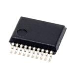
LTC2320IUKG-16#PBF
Part Number : LTC2320IUKG-16#PBF
Analog Devices Inc.Analog to Digital Converters - ADC Octal, 16-Bit, 1.5Msps/ch Simultaneous Sampling SAR ADC

PD57-2-1260-CANOPEN
Part Number : PD57-2-1260-CANOPEN
Analog Devices Inc.STEPPER MOTOR, 2-PH, 2.8A, 1.01N-M;
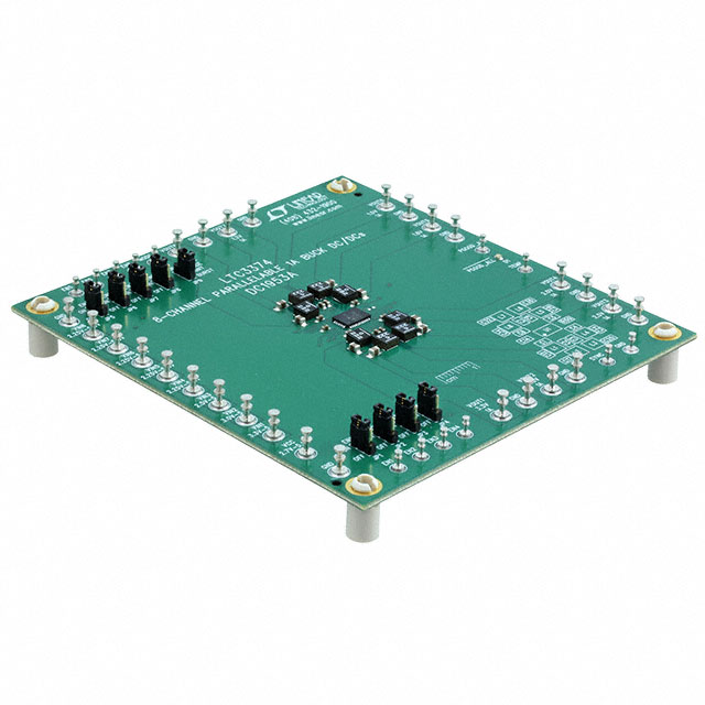
DC1953A
Part Number : DC1953A
Analog Devices Inc.Power Management IC Development Tools LTC3374EUHF Demo Board 8-Channel Parallelable 1A Buck DC/DC