MAX25612ATP/VY+T
Part Number : MAX25612ATP/VY+T
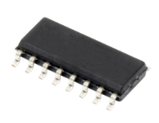
Analog Devices Inc.The MAX25612/MAX25612B is a single-channel high-brightness LED (HB LED) driver for automotive front-light applications such as high beam, low beam, daytime running light (DRL), turn indicator, fog light and other LED lights. It can take an input voltage from 5V to 48V and can drive a string of LEDs with a maximum output voltage of 65V. The MAX25612/MAX25612B is fully synchronous and is suitable for boost and buck-boost applications that need synchronous rectification providing efficiencies greater than 90%.The MAX25612/MAX25612B senses output current at the high side of the LED string. High-side current sensing is required to protect against shorts from the output to the ground or battery input. It is also the most flexible scheme for driving LEDs, allowing boost, high-side buck, or buck-boost mode configurations. The PWM input provides LED dimming ratios of up to 5000:1, and the ICTRL input provides additional analog dimming capability in the MAX25612/MAX25612B. The MAX25612/MAX25612B also includes a active-low FLT flag that indicates open string, shorted string, and thermal shutdown. The MAX25612/MAX25612B has built-in spread-spectrum modulation for improved electromagnetic compatibility performance. The MAX25612/MAX25612B is available in a space-saving (4mm x 4mm), 20-pin side-wettable TQFN or a 20-pin TSSOP package and is specified to operate overthe -40°C to +125°C automotive temperature range.ApplicationsAutomotive Exterior Lighting:Commercial, Industrial, and Architectural LightingDaytime Running Lights (DRLs)Fog Light and Adaptive Front-Light AssembliesHigh-Beam/Low-Beam/Signal/Position Lights
MAX25612BATP/VY+
Part Number : MAX25612BATP/VY+
Analog Devices Inc.The MAX25612/MAX25612B is a single-channel high-brightness LED (HB LED) driver for automotive front-light applications such as high beam, low beam, daytime running light (DRL), turn indicator, fog light and other LED lights. It can take an input voltage from 5V to 48V and can drive a string of LEDs with a maximum output voltage of 65V. The MAX25612/MAX25612B is fully synchronous and is suitable for boost and buck-boost applications that need synchronous rectification providing efficiencies greater than 90%.The MAX25612/MAX25612B senses output current at the high side of the LED string. High-side current sensing is required to protect against shorts from the output to the ground or battery input. It is also the most flexible scheme for driving LEDs, allowing boost, high-side buck, or buck-boost mode configurations. The PWM input provides LED dimming ratios of up to 5000:1, and the ICTRL input provides additional analog dimming capability in the MAX25612/MAX25612B. The MAX25612/MAX25612B also includes a active-low FLT flag that indicates open string, shorted string, and thermal shutdown. The MAX25612/MAX25612B has built-in spread-spectrum modulation for improved electromagnetic compatibility performance. The MAX25612/MAX25612B is available in a space-saving (4mm x 4mm), 20-pin side-wettable TQFN or a 20-pin TSSOP package and is specified to operate overthe -40°C to +125°C automotive temperature range.ApplicationsAutomotive Exterior Lighting:Commercial, Industrial, and Architectural LightingDaytime Running Lights (DRLs)Fog Light and Adaptive Front-Light AssembliesHigh-Beam/Low-Beam/Signal/Position Lights
MAX32666GXMBL+
Part Number : MAX32666GXMBL+
Analog Devices Inc.DARWIN is a new breed of low-power microcontrollers built to thrive in the rapidly evolving Internet of Things (IoT). They are smart, with the biggest memories in their class and a massively scalable memory architecture. They run forever, thanks to wearable-grade power technology. They are durable enough to withstand the most advanced cyberattacks. DARWIN microcontrollers are designed to run any application imaginable—in places where you would not dream of sending other microcontrollers.Generation UB microcontrollers are designed to handle the increasingly complex applications demanded by today's advanced battery-powered devices and wirelessly connected devices, while providing robust hardware security and Bluetooth® 5 Low Energy (BLE) radio connectivity.The MAX32665/MAX32666 UB class microcontrollers are advanced systems-on-chips featuring an Arm® Cortex®-M4 with FPU CPU for efficient computation of complex functions and algorithms with integrated power management. They also include the newest generation Bluetooth 5 Low Energy radio with high throughput (2Mbps) and Maxim's best-in-class hardware security suite trust protection unit (TPU). The devices offer large on-board memory with 1MB flash and up to 560KB SRAM that can be configured as 448KB SRAM with error correction coding (ECC). Split flash banks of 512KB each support seamless over the air upgrades, adding an additional degree of reliability. Memory scalability of data (SRAM) and code (flash) space is supported by two SPI execute-in-place (SPIX) interfaces.Multiple high-speed interfaces are supported including HS-USB, secure digital interface (SD, SDIO, MMC, SDHC, and microSD™), SPI, UART, and I2C serial interfaces, and an audio subsystem supporting PDM, PCM, I2S, and TDM interfaces. An 8-input, 10-bit ADC is available to monitor analog inputs from external sensors and meters. The devices are available in 109-bump WLP (0.35mm pitch) and 121-bump CTBGA (0.65mm pitch).ApplicationsConnected HomeGaming DevicesHearablesIndustrial SensorsPayment/Fitness/Medical WearablesTelemedicine
MAX33054EASA+T
Part Number : MAX33054EASA+T
Analog Devices Inc.The MAX33053E and MAX33054E are +3.3V CAN (Control Area Network) transceivers with integrated protection for industrial applications. These devices have extended ±65V fault protection for equipment where overvoltage protection is required. It also incorporates high ±25kV ESD HBM and an input common mode range (CMR) of ±25V, exceeding the ISO11898 specification of -2V to +7V. This makes these parts well-suited for applications that are in electrically noisy environments where the ground planes are shifting relative to each other. This family features a variety of options to address common CAN application requirements; logic-level supply input VL for interfacing with 1.62V to 3.6V logic, low-current standby mode, silent-mode to disable the transmitter, and a slow slew rate to minimize EMI.These devices operate at a high-speed CAN data rate, allowing up to 2Mbps on small networks. Maximum speed on large networks may be limited by the number of nodes in a network, the type of cabling used, stub length, and other factors. These transceivers include a dominant timeout to prevent bus lockup caused by controller error or by a fault on the TXD input. When TXD remains in the dominant state (low) for longer than TDOM, the driver is switched to the recessive state, releasing the bus. The MAX33053E features an S pin where it enables and disables the transmitter for applications where you need the transceiver to receive only. The MAX33054E features a STBY pin for 3 modes of operation; standby mode for low-current consumption, normal high-speed mode, or a slow slew rate mode when an external 26.1kΩ is connected between ground and STBY pin.The MAX33053E and MAX33054E are available in a standard 8-pin SOIC package and operate over the -40°C to +125°C temperature range.ApplicationsBuilding AutomationDroneIndustrial AutomationInstrumentationMotor ControlProgrammable Logic ControllerSmart Grid Equipment
MAX38912ATA+
Part Number : MAX38912ATA+
Analog Devices Inc.The MAX38911/MAX38912 are low-noise, high-PSRR PMOS linear regulators that deliver up to a 500mA load current with only 11µVRMS of output noise from 10Hz to 100kHz.The regulators are fully protected from damage by internal circuitry that provides programmable inrushcurrent limiting, output overcurrent limiting, reverse current limiting, and thermal overload protection.The MAX38911 is available in WLP and TDFN packages and are default factory preprogrammed to an output voltage of 1.8V. Custom fixed-output voltage levels in the range of 0.8V to 5.0V in 50mV steps are alsoavailable, see Ordering Information.MAX38912 provides enhanced flexibility with adjustable output voltage in the range of 0.8V to 5.0V by using twoexternal feedback resistors.The MAX38911ANT is packaged in a 1.42mm x 0.83mm, 3 x 2, 6-bump, 0.4mm pitch WLP, while the MAX38911ATA and MAX38912ATA are packaged in a 8-pin, 2mm x 2mm TDFN.ApplicationsDigital Camera and Audio DevicesHigh-Performance Sensors for Portable ApplicationsImaging and High-Frequency SensorsIoT SensorsMobile PhonesPortable and Battery-Powered Equipment
LTC3861EUH-1#PBF
Part Number : LTC3861EUH-1#PBF
Analog Devices Inc.The LTC3861-1 is a dual PolyPhase® synchronous stepdown switching regulator controller for high current distributed power systems, digital signal processors, and other telecom and industrial DC/DC power supplies. It uses a constant-frequency voltage mode architecture combined with very low offset, high bandwidth error amplifiers and a remote output sense differential amplifier for excellent transient response and output regulation.The controller incorporates lossless inductor DCR current sensing to maintain current balance between phases and to provide overcurrent protection. The chip operates from a VCC supply between 3V and 5.5V and is designed for stepdown conversion from VIN between 3V and 24V to output voltages between 0.6V and VCC – 0.5V.Inductor current reversal is disabled during soft-start to safely power prebiased loads. The constant operating frequency can be synchronized to an external clock or linearly programmed from 250kHz to 2.25MHz. Up to six LTC3861-1 controllers can operate in parallel for 1-, 2-, 3-, 4-, 6- or 12-phase operation.The LTC3861-1 is pin-to-pin compatible with the LTC3860. It is available in a 32-pin 5mm × 5mm QFN package. The LTC3861is a 36-pin QFN version of the LTC3861-1, which has dual differential output voltage sense amplifiers. # Diff Amps Config Pin Package LTC3861 2 Yes 5 x 6 QFN-36 LTC3861-1 1 No 5 x 5 QFN-32 Applications High Current Distributed Power Systems DSP, FPGA and ASIC Supplies Datacom and Telecom Systems Industrial Power Supplies
LTC3869IUF#PBF
Part Number : LTC3869IUF#PBF
Analog Devices Inc.The LTC3869 is a high performance dual synchronous step-down switching regulator controller that drives all N-channel synchronous power MOSFET stages. A constant frequency current mode architecture allows a phase-lockable frequency of up to 780kHz. Power loss and noise due to the ESR of the input capacitors are minimized by operating the two controller output stages out-of-phase.OPTI-LOOP® compensation allows the transient response to be optimized over a wide range of output capacitance and ESR values. A wide 4V to 38V input supply range encompasses most battery chemistries. Independent TK/SS pins for each controller ramp the output voltage during start-up. Current foldback limits MOSFET heat dissipation during short-circuit conditions. The MODE/PLLIN pin selects among Burst Mode® operation, pulse-skipping mode, or continuous inductor current mode and allows the IC to be synchronized to an external clock.The LTC3869 is available in low profile 4mm × 4mm and 4mm × 5mm QFN packages. The LTC3869-2 is available in an SSOP-28 package. The LTC3869 is pin-compatible with the LTC3850.Applications Server Systems Telecom Systems Industrial and Medical Instruments High Power Battery-Operated Devices DC Power Distribution Systems
LTC3890IUH-2#PBF
Part Number : LTC3890IUH-2#PBF
Analog Devices Inc.The LTC3890-2 is a high performance dual step-down switching regulator DC/DC controller that drives all N-channel synchronous power MOSFET stages. A constant frequency current mode architecture allows a phase-lockable frequency of up to 850kHz. Power loss and noise due to the ESR of the input capacitor are minimized by operating the two controller output stages out-of-phase.The 50μA no-load quiescent current extends operating run time in battery-powered systems. OPTI-LOOP® compensation allows the transient response to be optimized over a wide range of output capacitance and ESR values. A wide 4V to 60V input supply range encompasses a wide range of intermediate bus voltages and battery chemistries.Independent TRACK/SS pins for each controller ramp the output voltages during start-up. Current mode control limits the inductor current during short-circuit conditions. The PLLIN/MODE pin selects among Burst Mode operation, pulse-skipping mode, or continuous conduction mode at light loads. For versions with different and/or additional features, see the LTC3890 family summary, Table 1, in the Pin Functions section of this data sheet. LTC3890 LTC3890-1 LTC3890-2 LTC3890-3 Adjustable Current Limit Yes No Yes No CLKOUT/PHASMD for Multiphase Operation Yes No Yes No Number of PGood Outputs 2 1 2 1 OVP – Bottom Gate Crowbar Yes Yes No No Current Limit Foldback Yes Yes No No Light Load Operation when Synced to External Clock Forced Continuous Forced Continuous Pulse Skipping Pulse Skipping SENSE Pins Common Mode Range Common Mode < 0.5V Requires VFB < 0.65V Common Mode < 0.5V Requires VFB < 0.65V Not Dependant on VFB. Easy to make a non-synchronous Boost or SEPIC Not Dependant on VFB. Easy to make a non-synchronous Boost or SEPIC Package 5X5 QFN-32 SSOP-28 5X5 QFN-32 SSOP-28 Applications Automotive Always-On Systems Battery Operated Digital Devices Distributed DC Power Systems
LTC4000EUFD-1#PBF
Part Number : LTC4000EUFD-1#PBF
Analog Devices Inc.The LTC4000-1 is a high voltage, high performance controller that converts many externally compensated DC/DC power supplies into full-featured battery chargers with maximum power point control. In contrast to the LTC4000, the LTC4000-1 has an input voltage regulation loop instead of the input current regulation loop.Features of the LTC4000-1’s battery charger include: accurate (±0.25%) programmable float voltage, selectable timer or current termination, temperature qualified charging using an NTC thermistor, automatic recharge, C/10 trickle charge for deeply discharged cells, bad battery detection and status indicator outputs. The battery charger also includes precision current sensing that allows lower sense voltages for high current applications.The LTC4000-1 supports intelligent PowerPath control. An external PFET provides low loss reverse current protection. Another external PFET provides low loss charging or discharging of the battery. This second PFET also facilitates an instant-on feature that provides immediate downstream system power even when connected to a heavily discharged or shorted battery.The LTC4000-1 is available in a low profile 28-lead 4mm × 5mm QFN and SSOP packages. LTC4000 LTC4000-1 Input Voltage Regulation MPPC No Yes Input Current Monitoring Yes Yes Input Current Regulation Yes No Applications Solar Powered Battery Charger Systems Battery Charger with High Impedance Input Source, e.g., Fuel Cell or Wind Turbine Battery Equipped Industrial or Portable Military Equipments
LTC4270CIUKG#PBF
Part Number : LTC4270CIUKG#PBF
Analog Devices Inc.The LTC4270/LTC4271 chipset is a 12-port power sourcing equipment (PSE) controller designed for use in IEEE 802.3at Type 1 and Type 2 (high power) compliant Power over Ethernet (PoE) systems. Transformer-isolated communication protocol replaces expensive opto-couplers and complex isolated 3.3V supply resulting in significant BOM cost savings. The LTC4270/LTC4271 chipset delivers lowest-in-industry heat dissipation by utilizing low-RDS(ON) external MOSFETs and 0.25Ω sense resistors.Advanced power management features include per-port 12‑bit current monitoring ADCs, DAC-programmable current limit, and versatile fast shut-down of preselected ports. Advanced power management host software is available under a no-cost license. PD discovery uses a proprietary dual-mode 4-point detection mechanism ensuring excellent immunity from false PD detection. Midspan PSEs are supported with 2-event classification and a 2 second backoff timer. The LTC4270/LTC4271 includes an I2C serial interface operable up to 1MHz.The LTC4270/LTC4271 is available in multiple power grades allowing delivered PD power up to 90W.Applications PoE PSE Switches/Routers PoE PSE Midspans
LTC4366HDDB-1#TRMPBF
Part Number : LTC4366HDDB-1#TRMPBF
Analog Devices Inc.The LTC4366 surge stopper protects loads from high voltage transients. By controlling the gate of an external N-channel MOSFET, the LTC4366 regulates the output during an overvoltage transient. The load may remain operational while the overvoltage is dropped across the MOSFET. Placing a resistor in the return line isolates the LTC4366 and allows it to float up with the supply; therefore, the upper limit on the output voltage depends only on the availability of high valued resistors and MOSFET ratings.An adjustable overvoltage timer prevents MOSFET damage during the surge while an additional 9-second timer provides for MOSFET cool down. A shutdown pin reduces the quiescent current to less than 14μA during shutdown. After a fault the LTC4366-1 latches off while the LTC4366-2 will auto-retry.Applications Industrial, Automotive and Avionic Surge Protection High Voltage DC Distribution 28V Vehicle Systems
LTC5544IUF#PBF
Part Number : LTC5544IUF#PBF
Analog Devices Inc.The LTC5544 is part of a family of high dynamic range, high gain passive downconverting mixers covering the 600MHz to 6GHz frequency range. The LTC5544 is optimized for 4GHz to 6GHz RF applications. The LO frequency must fall within the 4.2GHz to 5.8GHz range for optimum performance. A typical application is a WiMAX receiver with a 5.15GHz to 5.35GHz RF input and low side LO.The LTC5544 is designed for 3.3V operation, however; the IF amplifier can be powered with 5V for the higher P1dB.The LTC5544’s high level of integration minimizes the total solution cost, board space and system-level variation, while providing the highest dynamic range for demanding receiver applications.Applications 5GHz WiMAX/WLAN Receiver 4.9GHz Public Safety Bands 4.9GHz to 6GHz Military Communications Point-to-Point Broadband Communications Radar Systems
LTM2892CY-I#PBF
Part Number : LTM2892CY-I#PBF
Analog Devices Inc.The LTM2892 is a complete galvanic digital μModule® (micromodule) isolator. No external components are required. Individual 3V to 5.5V supplies power each side of the digital isolator. Separate logic supply pins allow easy interfacing with different logic levels from 1.62V to 5.5V, independent of the main supply.Module options are available with compatibility to SPI (LTM2892-S) and I2C (LTM2892-I), master mode only, specifications.Coupled inductors provide 3500VRMS of isolation between the input and output logic interface. This device is ideal for systems where the ground loop is broken, allowing uninterrupted communication through large common mode transients faster than 50kV/μs.Applications Isolated SPI or I2C Interfaces Industrial Systems Test and Measurement Equipment Breaking Ground Loops
LTM9010CY-14#PBF
Part Number : LTM9010CY-14#PBF
Analog Devices Inc.The LTM9011-14/LTM9010-14/LTM9009-14 are 8-channel, simultaneous sampling 14-bit A/D converters designed for digitizing high frequency, wide dynamic range signals. AC performance includes 73.1dB SNR and 88dB spurious free dynamic range (SFDR). Low power consumption per channel reduces heat in high channel count applications. Integrated bypass capacitance and flow-through pinout reduces overall board space requirements.DC specs include ±1LSB INL (typ), ±0.3LSB DNL (typ) and no missing codes over temperature. The transition noise is a low 1.2LSBRMS.The digital outputs are serial LVDS to minimize the number of data lines. Each channel outputs two bits at a time (2-lane mode). At lower sampling rates there is a one bit per channel option (1-lane mode).The ENC+ and ENC– inputs may be driven differentially or single-ended with a sine wave, PECL, LVDS, TTL, or CMOS inputs. An internal clock duty cycle stabilizer allows high performance at full speed for a wide range of clock duty cycles.Applications Communications Cellular Base Stations Software Defined Radios Portable Medical Imaging Multichannel Data Acquisition Nondestructive Testing
LTP5900IPC-WHMA1B2#PBF
Part Number : LTP5900IPC-WHMA1B2#PBF
Analog Devices Inc.SmartMesh WirelessHART wireless sensor networks are self managing, low power networks built from wireless nodes called motes. The LTP5900-WHM is the 22-pin SmartMesh WirelessHART mote product in the Eterna® family of IEEE 802.15.4 printed circuit board assembly solutions, featuring a highly-integrated, low power radio design by Analog Devices as well as an ARM Cortex-M3 32-bit microprocessor running Analog Devices' embedded SmartMesh WirelessHART networking software.The LTP5900-WHM provides a forward compatible solution for customers using Analog Devices' M2510 PCB module. Also available are the LTP5901-WHM module with chip antenna and the LTP5902-WHM module with MMCX antenna connector.With Analog Devices' time-synchronized WirelessHART networks, all motes in the network may route, source or terminate data, while providing many years of battery powered operation. The SmartMesh WirelessHART software provided with the LTP5900-WHM is fully tested and validated, and is readily configured via a software Application Programming Interface (API).Network Features Features Benefit Time Synchronized Channel Hopping Communications >99.999% network reliability in even the most challenging RF environments. Sub 50 µA Routers Can build out a network without any line powered devices. Flexibility to be line powered or energy harvested if desired. Secure Mesh with 128-bit AES Encryption NIST Certified Security. Compromise of one node does not compromise network. Standards-based Compliant to IEC62591 (WirelessHART). Highly Accurate Time Stamping Time stamping on every node is available to applications with millisecond accuracy. Device Features Features Benefit Industry-Leading Low Power Radio Technology 4.5mA to Receive a Packet 5.4mA to Transmit at 0dBm 9.7mA to Transmit at 8dBm Pre-engineered RF RF elements include an on-chip power amplifier and are pre-tuned for optimized performance, including temperature compensation, saving development time. RF Modular Certifications Pre-certified in USA, Canada, and EU. Energy Harvesting Support Very low power design enables motes to be powered by a wide variety of energy harvesters. ApplicationsLearn more about SmartMesh applications.
MAX11040KGUU+
Part Number : MAX11040KGUU+
Analog Devices Inc.The MAX11040K/MAX11060 are 24-/16-bit, 4-channel, simultaneous-sampling, sigma-delta analog-to-digital converters (ADCs). The devices allow simultaneous sampling of as many as 32 channels using a built-in cascade feature to synchronize as many as eight devices. The serial interface of the devices allows reading data from all the cascaded devices using a single command. Four modulators simultaneously convert each fully differential analog input with a programmable data output rate ranging from 0.25ksps to 64ksps. The devices achieve 106dB SNR at 16ksps and 117dB SNR at 1ksps (MAX11040K). The devices operate from a single +3V supply. The differential analog input range is ±2.2V when using the internal reference; an external reference is optional. Each input is overvoltage protected up to ±6V without damage. The devices use an internal crystal oscillator or an external source for clock.The devices are compatible with SPI, QSPI™, MICROWIRE®, and DSP-compatible 4-wire serial interfaces. An on-board interface logic allows one serial interface (with a single chip select) to control up to eight cascaded devices or 32 simultaneous sampling analog input channels.The devices are ideally suited for power-management systems. Each channel includes an adjustable sampling phase enabling internal compensation for phase shift due to external dividers, transformers, or filters at the inputs. The output data rate is adjustable with a 0.065% resolution (at 16ksps or below) to track the varying frequency of a periodic input. An active-low SYNC input allows periodic alignment of the conversion timing of multiple devices with a remote timing source.The devices are available in a 38-pin TSSOP package specified over the -40°C to +105°C industrial temperature range.ApplicationsIndustrial Data-Acquisition SystemsMedical InstrumentationMultiphase Power SystemsPower-Protection Relay Equipment
MAX11338ATJ+
Part Number : MAX11338ATJ+
Analog Devices Inc.The MAX11335–MAX11340 are 12-/10-bit with external reference and 500kHz, full-linear-bandwidth, high-speed, low-power, serial-output successive approximation register (SAR) analog-to-digital converters (ADCs). MAX11335–MAX11340 provide external access to the output of the integrated mux and ADC input, to simplify conditioning. MAX11335–MAX11340 include both internal and external clock modes. These devices feature scan mode in both internal and external clock modes. The internal clock mode features internal averaging to increase SNR. The external clock mode features the SampleSet™ technology, a user-programmable analog input channel sequencer. The SampleSet approach provides greater sequencing flexibility for multichannel applications while alleviating significant microcontroller or DSP (controlling unit) communication overhead.External pins provide access to the output of the multiplexer and ADC inputs to simplify multichannel signal conditioning. The internal clock mode features an integrated FIFO allowing data to be sampled at high speeds and then held for readout at any time or at a lower clock rate. Internal averaging is also supported in internal clock mode improving SNR for noisy input signals. The devices feature analog input channels that can be configured to be single-ended inputs, fully differential pairs, or pseudo-differential inputs with respect to one common input. TheMAX11321–MAX11328 operate from a 2.35V to 3.6V supply and consume only 4.2mW at 500ksps.The MAX11335–MAX11340 include AutoShutdown™, fast wake-up, and a high-speed 3-wire serial interface. The devices feature full power-down mode for optimal power management. The 8MHz, 3-wire serial interface directly connects to SPI, QSPI™, and MICROWIRE® devices without external logic.Excellent dynamic performance, low voltage, low power, ease of use, and small package size make these converters ideal for portable battery-powered data-acquisition applications, and for other applications that demand low power consumption and small space.The MAX11335–MAX11340 are available in 32-pin, 5mm x 5mm, TQFN packages and operate over the -40°C to +125°C temperature range. ApplicationsBattery-Powered InstrumentsHigh-Speed Closed-Loop SystemsHigh-Speed Data Acquisition SystemsIndustrial Control SystemsMedical InstrumentationPortable Systems
MAX13256ATB+T
Part Number : MAX13256ATB+T
Analog Devices Inc.The MAX13256 H-bridge transformer driver provides a simple solution for making isolated power supplies up to 10W. The device drives a transformer's primary coil with up to 300mA of current from a wide 8V to 36V DC supply. The transformer's secondary-to-primary winding ratio defines the output voltage, allowing selection of virtually any isolated output voltage.The device features adjustable current limiting, allowing indirect limiting of secondary-side load currents. The current limit of the MAX13256 is set by an external resistor. An active-low FAULT output asserts when the device detects an overtemperature or overcurrent condition. In addition, the device features a low-power mode to reduce the overall supply current to 0.65mA (typ) when the driver is not in use.The device features an internal oscillator for autonomous operation and an external clock source input to synchronize multiple MAX13256 devices and precisely set the switching frequency. Internal circuitry guarantees a fixed 50% duty cycle to prevent DC current flow through the transformer, regardless of which clock source is used.The device is available in a small 10-pin (3mm x 3mm) TDFN package and is specified over the -40°C to +125°C automotive temperature range.Applications24V PLC Supply IsolationIsolated Fieldbus InterfacesMedical EquipmentMotor ControlsPower Meters
MAX14575AETA+T
Part Number : MAX14575AETA+T
Analog Devices Inc.The MAX14575A/MAX14575AL/MAX14575B/MAX14575C programmable current-limit switches feature internal current limiting to prevent damage to host devices due to faulty load conditions. These current-limit switches feature a low 32mΩ (typ) on-resistance and operate from a +2.3V to +5.5V input-voltage range. The current limit is adjustable from 250mA to 2.5A, making these devices ideal for charging a large load capacitor, as well as for high-current load switching applications. Each device in the family handles an overcurrent event differently depending on the option selected. The MAX14575A/MAX14575AL feature an autoretry mode; the MAX14575A has active-high EN polarity, while the MAX14575AL has active-low EN polarity. The MAX14575B has latch-off mode, and the MAX14575C features a continuous current-limit mode. Additional safety features include thermal-shutdown protection to prevent overheating and reverse-current blocking to prevent current from being driven back into the source. The MAX14575A/MAX14575AL/MAX14575B/MAX14575C are available in a small 2mm x 2mm, 8-pin TDFN package and operate over the -40°C to +85°C extended temperature range.ApplicationsData Modem CardsPortable Media PlayersRF Power Amplifier in Cell PhonesSDXC Card Power-Supply ProtectionUSB PortsUTCA/ATCA Platforms
MAX14575ALETA+T
Part Number : MAX14575ALETA+T
Analog Devices Inc.The MAX14575A/MAX14575AL/MAX14575B/MAX14575C programmable current-limit switches feature internal current limiting to prevent damage to host devices due to faulty load conditions. These current-limit switches feature a low 32mΩ (typ) on-resistance and operate from a +2.3V to +5.5V input-voltage range. The current limit is adjustable from 250mA to 2.5A, making these devices ideal for charging a large load capacitor, as well as for high-current load switching applications. Each device in the family handles an overcurrent event differently depending on the option selected. The MAX14575A/MAX14575AL feature an autoretry mode; the MAX14575A has active-high EN polarity, while the MAX14575AL has active-low EN polarity. The MAX14575B has latch-off mode, and the MAX14575C features a continuous current-limit mode. Additional safety features include thermal-shutdown protection to prevent overheating and reverse-current blocking to prevent current from being driven back into the source. The MAX14575A/MAX14575AL/MAX14575B/MAX14575C are available in a small 2mm x 2mm, 8-pin TDFN package and operate over the -40°C to +85°C extended temperature range.ApplicationsData Modem CardsPortable Media PlayersRF Power Amplifier in Cell PhonesSDXC Card Power-Supply ProtectionUSB PortsUTCA/ATCA Platforms


