
LTC2632HTS8-LX8#TRPBF
Part Number : LTC2632HTS8-LX8#TRPBF
Analog Devices Inc.The LTC2632 is a family of dual 12-, 10-, and 8-bit voltage-output DACs with an integrated, high-accuracy, low-drift reference in an 8-lead TSOT-23 package. It has rail-to-rail output buffers and is guaranteed monotonic.The LTC2632-L has a full-scale output of 2.5V, and operates from a single 2.7V to 5.5V supply. The LTC2632-H has a full-scale output of 4.096V, and operates from a 4.5V to 5.5V supply. Each DAC can also operate with an external reference, which sets the full-scale output to the external reference voltage.These DACs communicate via a simple SPI/MICROWIRE compatible 3-wire serial interface which operates at clock rates up to 50MHz. The LTC2632 incorporates a power-on reset circuit. Options are available for reset to zero-scale or reset to mid-scale in internal reference mode, or reset to mid-scale in external reference mode after power-up.Applications Mobile Communications Process Control and Industrial Automation Automatic Test Equipment Portable Equipment Automotive

LTC2960HTS8-1#TRMPBF
Part Number : LTC2960HTS8-1#TRMPBF
Analog Devices Inc.The LTC2960 is a nano-current, high voltage two-input voltage monitor, ideally suited for multicell battery applications. External resistive dividers configure custom comparator thresholds. The supervisory circuit monitors the ADJ input and pulls the RST output low when the input drops below threshold. A reset timeout period delays the return of the RST output to a high state when the input rises above the threshold. The spare comparator allows voltage conditions to be detected with either a non-inverting input, IN+ (LTC2960-1/LTC2960-3) or an inverting input, IN– (LTC2960-2/LTC2960-4). A manual reset (MR) input is provided for external activation of the reset output.Other options provided on the LTC2960-1/LTC2960-2 include a reset timeout period select pin, RT, to select between 15ms or 200ms reset timeout periods. The LTC2960-3/LTC2960-4 have a fixed 200ms reset timeout period. The RST and OUT outputs are available with active pull-up circuits to an output logic supply pin (LTC2960-3/LTC2960-4) or 36V open-drain outputs (LTC2960-1/LTC2960-2).Applications Portable Equipment Battery Powered Equipment Security Systems Automotive Systems
LTC2960ITS8-3#TRMPBF
Part Number : LTC2960ITS8-3#TRMPBF
Analog Devices Inc.The LTC2960 is a nano-current, high voltage two-input voltage monitor, ideally suited for multicell battery applications. External resistive dividers configure custom comparator thresholds. The supervisory circuit monitors the ADJ input and pulls the RST output low when the input drops below threshold. A reset timeout period delays the return of the RST output to a high state when the input rises above the threshold. The spare comparator allows voltage conditions to be detected with either a non-inverting input, IN+ (LTC2960-1/LTC2960-3) or an inverting input, IN– (LTC2960-2/LTC2960-4). A manual reset (MR) input is provided for external activation of the reset output.Other options provided on the LTC2960-1/LTC2960-2 include a reset timeout period select pin, RT, to select between 15ms or 200ms reset timeout periods. The LTC2960-3/LTC2960-4 have a fixed 200ms reset timeout period. The RST and OUT outputs are available with active pull-up circuits to an output logic supply pin (LTC2960-3/LTC2960-4) or 36V open-drain outputs (LTC2960-1/LTC2960-2).Applications Portable Equipment Battery Powered Equipment Security Systems Automotive Systems

LTC2996CDD#PBF
Part Number : LTC2996CDD#PBF
Analog Devices Inc.The LTC2996 is a high accuracy temperature sensor with adjustable overtemperature and undertemperature thresholds and open drain alert outputs. It converts the temperature of an external diode sensor or its own die temperature to an analog output voltage while rejecting errors due to noise and series resistance. The measured temperature is compared against upper and lower limits set with resistive dividers. If a threshold is exceeded, the device communicates an alert by pulling low the correspondent open drain logic output.The LTC2996 gives ±1°C accurate temperature results using commonly available NPN or PNP transistors or temperature diodes built into modern digital devices. A 1.8V reference output simplifies threshold programming and can be used as an ADC reference input.The LTC2996 provides an accurate, low power solution for temperature monitoring in a compact 3mm × 3mm DFN package.Applications Temperature Monitoring and Measurement System Thermal Control Network Servers Desktop and Notebook Computers Environmental Monitoring

LTC3255EDD#PBF
Part Number : LTC3255EDD#PBF
Analog Devices Inc.The LTC3255 is a switched-capacitor step-down DC/DC converter that produces a regulated output (2.4V to 12.5V adjustable) from a 4V to 48V input. In applications where the input voltage exceeds twice the output voltage, 2:1 capacitive charge pumping extends output current capability beyond input supply current limits. At no load, Burst Mode® operation cuts VIN quiescent current to 16μA.With its integrated VIN shunt regulator, the LTC3255 excels in 4mA to 20mA current loop applications. The device enables current multiplication; a 4mA input current can power a 7.4mA load continuously. Alternatively, the LTC3255 serves as a higher efficiency replacement for linear regulators and provides a space-saving inductorfree alternative to buck DC/DC converters.The LTC3255 withstands reverse-polarity input supplies and output short-circuits without damage. Safety features including current limit and overtemperature protection further enhance robustness. The LTC3255 is available in thermally enhanced 10-lead MSOP and low profile 3mm × 3mm 10-lead DFN packages.Applications Industrial Control, Factory Automation, Sensors, and SCADA Systems Housekeeping Power Supplies Current-Boosting Voltage Regulators for 4mA to 20mA Current Loops

LTC3621HMS8E-25#PBF
Part Number : LTC3621HMS8E-25#PBF
Analog Devices Inc.The LTC3621/LTC3621-2 is a high efficiency 17V, 1A synchronous monolithic step-down regulator. The switching frequency is fixed to 1MHz or 2.25MHz with a ±40% synchronizing range. The regulator features ultralow quiescent current and high efficiencies over a wide VOUT range.The step-down regulator operates from an input voltage range of 2.7V to 17V and provides an adjustable output range from 0.6V to VIN while delivering up to 1A of output current. A user-selectable mode input is provided to allow the user to trade off ripple noise for light load efficiency; Burst Mode operation provides the highest efficiency at light loads, while pulse-skipping mode provides the lowest voltage ripple. The MODE pin can also be used to allow the user to sync the switching frequency to an external clock. LTC3621 Options Part Name Frequency VOUT LTC3621 1.00MHz Adjustable LTC3621-3.3 1.00MHz 3.3V LTC3621-5 1.00MHz 5V LTC3621-2 2.25MHz Adjustable LTC3621-23.3 2.25MHz 3.3 LTC3621-25 2.25MHz 5V APPLICATIONS Portable-Handheld Scanners Industrial and Embedded Computing Automotive Applications Emergency Radio
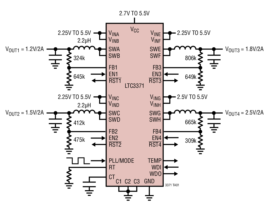
LTC3371IFE#PBF
Part Number : LTC3371IFE#PBF
Analog Devices Inc.The LTC3371 is a highly flexible multi-output power supply IC. The device includes four synchronous buck converters, configured to share eight 1A power stages, each of which is powered from independent 2.25V to 5.5V inputs.The DC/DCs are assigned to one of eight possible power configurations via pin programmable C1-C3 pins. The common buck switching frequency may be programmed with an external resistor, synchronized to an external oscillator, or set to a default internal 2MHz clock. The operating mode for all DC/DCs may be programmed for Burst Mode or forced continuous mode operation.The CT pin programs the timing parameters of four independent RST pins as well as the watchdog timer.To reduce input noise, the buck converters are phased in 90° steps. Precision enable pin thresholds facilitate reliable power sequencing. The LTC3371 is available in low profile 38-lead 5mm × 7mm QFN and TSSOP packages.Applications General Purpose Multichannel Power Supplies: Automotive, Industrial, Distributed Power Systems

LTC3622HDE-2#PBF
Part Number : LTC3622HDE-2#PBF
Analog Devices Inc.The LTC3622 is a dual 1A output, high efficiency synchronous monolithic step-down regulator capable of operating from input supplies up to 17V. The switching frequency is fixed to 1MHz or 2.25MHz with a ±50% synchronization range to an external clock. The regulator features ultralow quiescent current and high efficiency over a wide output voltage range.The step-down regulators operate from an input voltage range of 2.7V to 17V and provide an adjustable output from 0.6V to VIN while delivering up to 1A of output current. A user-selectable mode input is provided to allow the user to trade off ripple noise for light load efficiency. Burst Mode® operation provides the highest efficiency at light loads, while pulse-skipping mode provides the lowest ripple noise. The switching regulators can be synchronized to an external clock. Furthermore, fixed VOUT options are available to eliminate the external feedback resistors. LTC3622 Options Part Name Frequency VOUT LTC3622 1.00MHz Adjustable LTC3622-2 2.25MHz Adjustable LTC3622-23/5 2.25MHZ 5V/3.3V Applications Battery Powered Systems Point-of-Load Supplies Portable – Handheld Scanners

LTC3769HFE#PBF
Part Number : LTC3769HFE#PBF
Analog Devices Inc.LTC3769 is a high performance single output synchronous boost converter controller that drives an all N-channel power MOSFET stage. Synchronous rectification increases efficiency, reduces power losses and eases thermal requirements, simplifying high power boost applications. The 28μA no-load quiescent current extends operating run time in battery-powered systems.A 4.5V to 60V input supply range encompasses a wide range of system architectures and battery chemistries. When biased from the output of the boost converter or another auxiliary supply, the LTC3769 can operate from an input supply as low as 2.3V after start-up. The operating frequency can be set within a 50kHz to 900kHz range or synchronized to an external clock using the internal PLL.The SS pin ramps the output voltage during start-up. The PLLIN/MODE pin selects Burst Mode® operation, pulse-skipping mode or forced continuous mode at light loads.APPLICATIONS Industrial Automotive Medical Military

LTC3899EFE#PBF
Part Number : LTC3899EFE#PBF
Analog Devices Inc.The LTC3899 is a high performance triple output (buck/ buck/boost) DC/DC switching regulator controller that drives all N-channel synchronous power MOSFET stages. The constant frequency current mode architecture allows a phase-lockable frequency of up to 850kHz. The LTC3899 operates from a wide 4.5V to 60V input supply range. When biased from the output of the boost converter or another auxiliary supply, the LTC3899 can operate from an input supply as low as 2.2V after start-up.The gate drive for the LTC3899 can be programmed from 5V to 10V to allow the use of logic-level or standard-level FETs and to maximize efficiency. Internal switches in the top gate drivers eliminate the need for external bootstrap diodes. The 29μA no-load quiescent current extends operating run time in battery-powered systems. OPTI-LOOP® compensation allows the transient response to be optimized over a wide range of output capacitance and ESR values.APPLICATIONS Automotive Always-On and Start-Stop Systems Distributed DC Power Systems Multioutput Buck-Boost Applications
LTC3899IUHF#PBF
Part Number : LTC3899IUHF#PBF
Analog Devices Inc.The LTC3899 is a high performance triple output (buck/ buck/boost) DC/DC switching regulator controller that drives all N-channel synchronous power MOSFET stages. The constant frequency current mode architecture allows a phase-lockable frequency of up to 850kHz. The LTC3899 operates from a wide 4.5V to 60V input supply range. When biased from the output of the boost converter or another auxiliary supply, the LTC3899 can operate from an input supply as low as 2.2V after start-up.The gate drive for the LTC3899 can be programmed from 5V to 10V to allow the use of logic-level or standard-level FETs and to maximize efficiency. Internal switches in the top gate drivers eliminate the need for external bootstrap diodes. The 29μA no-load quiescent current extends operating run time in battery-powered systems. OPTI-LOOP® compensation allows the transient response to be optimized over a wide range of output capacitance and ESR values.APPLICATIONS Automotive Always-On and Start-Stop Systems Distributed DC Power Systems Multioutput Buck-Boost Applications
LTC3899MPUHF#PBF
Part Number : LTC3899MPUHF#PBF
Analog Devices Inc.The LTC3899 is a high performance triple output (buck/ buck/boost) DC/DC switching regulator controller that drives all N-channel synchronous power MOSFET stages. The constant frequency current mode architecture allows a phase-lockable frequency of up to 850kHz. The LTC3899 operates from a wide 4.5V to 60V input supply range. When biased from the output of the boost converter or another auxiliary supply, the LTC3899 can operate from an input supply as low as 2.2V after start-up.The gate drive for the LTC3899 can be programmed from 5V to 10V to allow the use of logic-level or standard-level FETs and to maximize efficiency. Internal switches in the top gate drivers eliminate the need for external bootstrap diodes. The 29μA no-load quiescent current extends operating run time in battery-powered systems. OPTI-LOOP® compensation allows the transient response to be optimized over a wide range of output capacitance and ESR values.APPLICATIONS Automotive Always-On and Start-Stop Systems Distributed DC Power Systems Multioutput Buck-Boost Applications

LTC4233CWHH#TRPBF
Part Number : LTC4233CWHH#TRPBF
Analog Devices Inc.The LTC4233 is an integrated solution for Hot Swap™ applications that allows a board to be safely inserted and removed from a live backplane. The part integrates a Hot Swap controller, power MOSFET and current sense resistor in a single package for small form factor applications. The MOSFET Safe Operating Area is production tested and guaranteed for the stresses in Hot Swap applications.The LTC4233 provides separate inrush current control and an 11% accurate 11.2A current limit with output dependent foldback. The current limit threshold can be adjusted dynamically using the ISET pin. Additional features include a current monitor output that amplifies the sense resistor voltage for ground referenced current sensing and a MOSFET temperature monitor output. Thermal limit, overvoltage, undervoltage and power good monitoring are also provided. For a 20A pin compatible version see LTC4234.Applications High Availability Servers Solid State Drives Industrial Network Routers and Switches

LTC4235IUFD-1#PBF
Part Number : LTC4235IUFD-1#PBF
Analog Devices Inc.The LTC4235 offers ideal diode-OR and Hot Swap™ functions for two 12V power rails by controlling external N-channel MOSFETs. MOSFETs acting as ideal diodes replace two high power Schottky diodes and the associated heat sinks, saving power and board area. A Hot Swap control MOSFET allows a board to be safely inserted and removed from a live backplane by limiting inrush current. The supply output is also protected against short-circuit faults with a foldback current limit and circuit breaker.The LTC4235 regulates the forward voltage drop across the MOSFETs to ensure smooth current transfer from one supply to the other without oscillation. The ideal diodes turn on quickly to reduce the load voltage droop during supply switchover. If the input supply fails or is shorted, a fast turn-off minimizes reverse-current transients.A current sense amplifier translates the voltage across the sense resistor to a ground referenced signal. The LTC4235 allows turn-on/off control, and reports fault and power good status for the supply.Applications Redundant Power Supplies High Availability Systems and Servers Telecom and Network Infrastructure

LTC4380CDD-1#PBF
Part Number : LTC4380CDD-1#PBF
Analog Devices Inc.The LTC4380 low quiescent current surge stopper protects loads from high voltage transients. Overvoltage protection is provided by clamping the gate voltage of an external N-channel MOSFET to limit the output voltage to a safe value during overvoltage events such as load dump in automobiles. Fixed gate clamp voltages are selectable for 12V and 24V/28V systems. For systems of any voltage up to 72V, use the adjustable gate clamp versions. Overcurrent protection is also provided.An internal multiplier generates a TMR pin current proportional to VDS and ID, so that operating time in both overcurrent and overvoltage conditions is limited in accordance with MOSFET stress.The GATE pin can drive back-to-back MOSFETs for reverse input protection, eliminating the voltage drop and dissipation of a Schottky diode solution. A low 8µA operating current permits use in always-on and battery powered applications. An accurate ON pin comparator monitors the input supply for undervoltage (UV) conditions and also serves as a shutdown input, reducing the quiescent current to 6µA.Applications Automotive/Avionic/Industrial Surge Protection Hot Swap, Live Insertion High Side Switch for Battery Powered Systems Automotive Load Dump Protection
LTC4380CDD-4#PBF
Part Number : LTC4380CDD-4#PBF
Analog Devices Inc.The LTC4380 low quiescent current surge stopper protects loads from high voltage transients. Overvoltage protection is provided by clamping the gate voltage of an external N-channel MOSFET to limit the output voltage to a safe value during overvoltage events such as load dump in automobiles. Fixed gate clamp voltages are selectable for 12V and 24V/28V systems. For systems of any voltage up to 72V, use the adjustable gate clamp versions. Overcurrent protection is also provided.An internal multiplier generates a TMR pin current proportional to VDS and ID, so that operating time in both overcurrent and overvoltage conditions is limited in accordance with MOSFET stress.The GATE pin can drive back-to-back MOSFETs for reverse input protection, eliminating the voltage drop and dissipation of a Schottky diode solution. A low 8µA operating current permits use in always-on and battery powered applications. An accurate ON pin comparator monitors the input supply for undervoltage (UV) conditions and also serves as a shutdown input, reducing the quiescent current to 6µA.Applications Automotive/Avionic/Industrial Surge Protection Hot Swap, Live Insertion High Side Switch for Battery Powered Systems Automotive Load Dump Protection

LTC4420IMSE#PBF
Part Number : LTC4420IMSE#PBF
Analog Devices Inc.The LTC4420 is a dual input monolithic PowerPath™ prioritizer, with low operating current, that provides backup switchover for keeping critical circuitry alive during brownout and power loss conditions. Unlike diode-OR products, little current is drawn from the inactive supply even if its voltage is greater than the active supply.Internal 2Ω, current limited PMOS switches provide power path selection from a primary input (V1) or a backup input (V2) to the output. Two adjustable voltage monitors set via external resistive dividers provide flexibility in setting V1 to V2 switchover and V2 undervoltage thresholds. V1 is monitored continuously while V2 supply monitoring includes controllable low duty cycle UV monitoring. When primary input V1 drops, the ADJ monitor causes OUT to be switched to V2. When V2 drops, it is disconnected from OUT if V2DIS is low. Fast non-overlap switchover circuitry prevents reverse and cross conduction while minimizing output droop.Auxiliary voltage monitor CMP1 provides flexible voltage monitoring and output V2OK provides V2 undervoltage status. Freshness seal mode prevents V2 battery discharge during storage or shipment.Applications Low Power Battery Backup Portable Equipment Point-of-Sale (POS) Equipment

LTC5548IUDB#TRPBF
Part Number : LTC5548IUDB#TRPBF
Analog Devices Inc.The LTC5548 is a high performance, microwave double balanced passive mixer that can be used for frequency upconversion or downconversion. The device is similar to the LTC5549, but with a broadband, differential DC to 6GHz IF port. The LTC5548 is recommended for applications where the IF frequency range extends below 500MHz. For applications where the IF frequency is always above 500MHz, the LTC5549 is recommended, since it includes an integrated IF balun.The LTC5548’s mixer and integrated RF balun are optimized to cover the 2GHz to 14GHz RF frequency range. The device includes an integrated LO amplifier optimized for the 1GHz to 12GHz frequency range, requiring only 0dBm drive. The device also includes an integrated LO frequency doubler, which can be enabled or disabled with a CMOS-compatible control pin.The LTC5548 delivers exceptionally high IIP3 and P1dB, in addition to very low LO to RF and LO to IF leakages. The part also offers high integration in a small package.Applications Microwave Transceivers Wireless Backhaul Point-to-Point Microwave Phased-Array Antennas C, X and Ku Band RADAR Test Equipment Satellite MODEMs

LTC6259HDC#TRMPBF
Part Number : LTC6259HDC#TRMPBF
Analog Devices Inc.The LTC6258/LTC6259/LTC6260 are single/dual/quad operational amplifiers with low noise, low power, low supply voltage, and rail-to-rail inputs and outputs. They are unity gain stable with or without capacitive loads. They feature 1.3MHz gain-bandwidth product, 0.24V/μs slew rate while consuming only 20μA of supply current per amplifier operating on supply voltages ranging from 1.8V to 5.25V. The combination of low supply current, low supply voltage, high gain bandwidth product and low noise makes the LTC6258 family unique among rail-to-rail input/output op amps with similar supply current. These operational amplifiers are ideal for power efficient applications.For applications that require power-down, the LTC6258 in 2mm × 2mm DFN and LTC6259 MS10 packages respectively offer shutdown which reduces the current consumption to 7μA maximum.The LTC6258 family can be used as plug-in replacements for many commercially available op amps to reduce power and improve input/output range and performance.Applications Micropower Active Filters Portable Instrumentation Battery or Solar Powered Systems Automotive Electronics

MAX4639EUE+
Part Number : MAX4639EUE+
Analog Devices Inc.The MAX4638/MAX4639 are single 8:1 and dual 4:1 CMOS analog multiplexers/demultiplexers (muxes/demuxes). Each mux operates from a single +1.8V to +5V supply or dual ±2.5V supplies. These devices feature 3.5Ω on-resistance (RON) when powered with a single +5V supply and have -75dB off-isolation and -85dB crosstalk from the output to each off channel. The switching times are 18ns tON and 7ns tOFF. They feature a -3dB 85MHz bandwidth and a guaranteed 0.25nA leakage current at +25°C. A +1.8V to +5.5V operating range makes the MAX4638/MAX4639 ideal for battery-powered, portable instruments. All channels guarantee break-before-make switching. These parts feature bidirectional operation and can handle rail-to-rail analog signals. All control inputs are TTL/CMOS-logic compatible. Decoding is in standard BCD format, and an enable input is provided to simplify cascading of devices. These devices are available in small 16-pin thin QFN, TSSOP, and SO packages, as well as a 20-pin TQFN package.ApplicationsAudio/Video Signal RoutingAutomated Test Equipment (ATE)Battery-Powered EquipmentLow-Voltage Data-Acquisition SystemsMedical EquipmentRelay Replacement


