
MAX16834ATP/V+
Part Number : MAX16834ATP/V+
Analog Devices Inc.The MAX16834 is a current-mode high-brightness LED (HB LED) driver for boost, boost-buck, SEPIC, and high-side buck topologies. In addition to driving an n-channel power MOSFET switch controlled by the switching controller, it also drives an n-channel PWM dimming switch to achieve LED PWM dimming. The MAX16834 integrates all the building blocks necessary to implement a fixed-frequency HB LED driver with wide-range dimming control. The MAX16834 features constant-frequency peak current-mode control with programmable slope compensation to control the duty cycle of the PWM controller.A dimming driver designed to drive an external n-channel MOSFET in series with the LED string provides wide-range dimming control up to 20kHz. In addition toPWM dimming, the MAX16834 provides analog dimming using a DC input at REFI. The programmable switching frequency (100kHz to 1MHz) allows design optimization for efficiency and board space reduction. A single resistor from RT/SYNC to ground sets the switching frequency from 100kHz to 1MHz while an external clock signal at RT/SYNC disables the internal oscillator and allows the MAX16834 to synchronize to an external clock. The MAX16834's integrated high-side current-sense amplifier eliminates the need for a separate high-side LED current-sense amplifier in boost-buck applications.The MAX16834 operates over a wide supply range of 4.75V to 28V and includes a 3A sink/source gate driver for driving a power MOSFET in high-power LED driverapplications. It can also operate at input voltages greater than 28V in boost configuration with an external voltage clamp. The MAX16834 is also suitable for DC-DC converter applications such as boost or buck-boost. Additional features include external enable/disable input, an on-chip oscillator, fault indicator output (active-low FLT) for LED open/short or overtemperature conditions, and an overvoltage protection sense input (OVP+) for true overvoltage protection.The MAX16834 is available in a thermally enhanced 4mm x 4mm, 20-pin TQFN-EP package and in a thermally enhanced 20-pin TSSOP-EP package and is specified over the automotive -40°C to +125°C temperature range.ApplicationsArchitectural and Decorative Lighting (MR16, MR111)Automotive Rear and Front LightingDC-DC Boost/Boost-Buck ConvertersProjection System RGB LED Light SourcesSingle-String LED LCD BacklightingSpot and Ambient Lights
MAX16834AUP+
Part Number : MAX16834AUP+
Analog Devices Inc.The MAX16834 is a current-mode high-brightness LED (HB LED) driver for boost, boost-buck, SEPIC, and high-side buck topologies. In addition to driving an n-channel power MOSFET switch controlled by the switching controller, it also drives an n-channel PWM dimming switch to achieve LED PWM dimming. The MAX16834 integrates all the building blocks necessary to implement a fixed-frequency HB LED driver with wide-range dimming control. The MAX16834 features constant-frequency peak current-mode control with programmable slope compensation to control the duty cycle of the PWM controller.A dimming driver designed to drive an external n-channel MOSFET in series with the LED string provides wide-range dimming control up to 20kHz. In addition toPWM dimming, the MAX16834 provides analog dimming using a DC input at REFI. The programmable switching frequency (100kHz to 1MHz) allows design optimization for efficiency and board space reduction. A single resistor from RT/SYNC to ground sets the switching frequency from 100kHz to 1MHz while an external clock signal at RT/SYNC disables the internal oscillator and allows the MAX16834 to synchronize to an external clock. The MAX16834's integrated high-side current-sense amplifier eliminates the need for a separate high-side LED current-sense amplifier in boost-buck applications.The MAX16834 operates over a wide supply range of 4.75V to 28V and includes a 3A sink/source gate driver for driving a power MOSFET in high-power LED driverapplications. It can also operate at input voltages greater than 28V in boost configuration with an external voltage clamp. The MAX16834 is also suitable for DC-DC converter applications such as boost or buck-boost. Additional features include external enable/disable input, an on-chip oscillator, fault indicator output (active-low FLT) for LED open/short or overtemperature conditions, and an overvoltage protection sense input (OVP+) for true overvoltage protection.The MAX16834 is available in a thermally enhanced 4mm x 4mm, 20-pin TQFN-EP package and in a thermally enhanced 20-pin TSSOP-EP package and is specified over the automotive -40°C to +125°C temperature range.ApplicationsArchitectural and Decorative Lighting (MR16, MR111)Automotive Rear and Front LightingDC-DC Boost/Boost-Buck ConvertersProjection System RGB LED Light SourcesSingle-String LED LCD BacklightingSpot and Ambient Lights
MAX16834AUP/V+
Part Number : MAX16834AUP/V+
Analog Devices Inc.The MAX16834 is a current-mode high-brightness LED (HB LED) driver for boost, boost-buck, SEPIC, and high-side buck topologies. In addition to driving an n-channel power MOSFET switch controlled by the switching controller, it also drives an n-channel PWM dimming switch to achieve LED PWM dimming. The MAX16834 integrates all the building blocks necessary to implement a fixed-frequency HB LED driver with wide-range dimming control. The MAX16834 features constant-frequency peak current-mode control with programmable slope compensation to control the duty cycle of the PWM controller.A dimming driver designed to drive an external n-channel MOSFET in series with the LED string provides wide-range dimming control up to 20kHz. In addition toPWM dimming, the MAX16834 provides analog dimming using a DC input at REFI. The programmable switching frequency (100kHz to 1MHz) allows design optimization for efficiency and board space reduction. A single resistor from RT/SYNC to ground sets the switching frequency from 100kHz to 1MHz while an external clock signal at RT/SYNC disables the internal oscillator and allows the MAX16834 to synchronize to an external clock. The MAX16834's integrated high-side current-sense amplifier eliminates the need for a separate high-side LED current-sense amplifier in boost-buck applications.The MAX16834 operates over a wide supply range of 4.75V to 28V and includes a 3A sink/source gate driver for driving a power MOSFET in high-power LED driverapplications. It can also operate at input voltages greater than 28V in boost configuration with an external voltage clamp. The MAX16834 is also suitable for DC-DC converter applications such as boost or buck-boost. Additional features include external enable/disable input, an on-chip oscillator, fault indicator output (active-low FLT) for LED open/short or overtemperature conditions, and an overvoltage protection sense input (OVP+) for true overvoltage protection.The MAX16834 is available in a thermally enhanced 4mm x 4mm, 20-pin TQFN-EP package and in a thermally enhanced 20-pin TSSOP-EP package and is specified over the automotive -40°C to +125°C temperature range.ApplicationsArchitectural and Decorative Lighting (MR16, MR111)Automotive Rear and Front LightingDC-DC Boost/Boost-Buck ConvertersProjection System RGB LED Light SourcesSingle-String LED LCD BacklightingSpot and Ambient Lights

MAX17075ETG+
Part Number : MAX17075ETG+
Analog Devices Inc.The MAX17075 includes a high-voltage boost regulator,one high-current operational amplifier, two regulated charge pumps, and one MLG block for gate-driver supply modulation.The step-up DC-DC converter is a 1.2MHz current-mode boost regulator with a built-in power MOSFET. It provides fast load-transient response to pulsed loads while producing efficiencies over 85%. The built-in 160mΩ (typ) power MOSFET allows output voltages as high as 18V boosted from inputs ranging from 2.5V to 5.5V. A built-in 7-bit digital soft-start function controls startup inrush currents.The gate-on and gate-off charge pumps provide regulated TFT gate-on and gate-off supplies. Both output voltages can be adjusted with external resistive voltage-dividers.The operational amplifier, typically used to drive the LCD backplane (VCOM), features high-output short-circuit current (±500mA), fast slew-rate (45V/µs), wide bandwidth (20MHz), and rail-to-rail outputs.The MAX17075 is available in a 24-pin thin QFN package with 0.5mm lead spacing. The package is a square (4mm x 4mm) with a maximum thickness of 0.8mm for ultra-thin LCD design. It operates over the -40°C to +105°C temperature range.ApplicationsLCD Monitor PanelsLCD TVsNotebook Computer Displays

MAX4993EVB+
Part Number : MAX4993EVB+
Analog Devices Inc.The MAX4991–MAX4994 low on-resistance analog switches operate from a single +1.8V to +5.5V supply. The MAX4991/MAX4993 feature a slow turn-on time to reduce clicks and pops due to coupling capacitors and audio amplifiers with a DC output bias. This feature provides click-and-pop reduction without adding additional parts for existing architectures.The MAX4991/MAX4992 are dual single-pole/double-throw (SPDT) switches, while the MAX4993/MAX4994 are double-pole/double-throw (DPDT) switches. The MAX4993/MAX4994 feature an active-low enable input (active-low EN) that sets all the channels to high impedance and reduces supply current when driven high. These devices have 0.3Ω on-resistance and 0.004% THD+N to route high fidelity audio signals.The MAX4991–MAX4994 are available in space-saving 10-pin UTQFN (1.4mm x 1.8mm) package, and are specified for operation over the -40°C to +85°C extended temperature range.ApplicationsAudio Signal RoutingCellular PhonesPortable MP3 PlayersSpeaker Headset Source Switching

MAX5137GTG+
Part Number : MAX5137GTG+
Analog Devices Inc.The MAX5134–MAX5137 is a family of pin-compatible and software-compatible 16-bit and 12-bit DACs. The MAX5134/MAX5135 are low-power, quad 16-/12-bit, buffered voltage-output, high-linearity DACs. The MAX5136/MAX5137 are low-power, dual 16-/12-bit, buffered voltage-output, high-linearity DACs. They use a precision internal reference or a precision external reference for rail-to-rail operation. The MAX5134–MAX5137 accept a wide +2.7V to +5.25V supply-voltage range to accommodate most low-power and low-voltage applications. These devices accept a 3-wire SPI-/QSPI™-/MICROWIRE®-/DSP-compatible serial interface to save board space and reduce the complexity of optically isolated and transformer-isolated applications. The digital interface’s double-buffered hardware and software active-low LDAC provide simultaneous output updates. The serial interface features an active-low READY output for easy daisy-chaining of several MAX5134–MAX5137 devices and/or other compatible devices. The MAX5134–MAX5137 include a hardware input to reset the DAC outputs to zero or midscale upon power-up or reset, providing additional safety for applications that drive valves or other transducers that need to be off during power-up. The high linearity of the DACs makes these devices ideal for precision control and instrumentation applications. The MAX5134–MAX5137 are available in an ultra-small (4mm x 4mm), 24-pin TQFN package or a 16-pin TSSOP package. Both packages are specified over the -40°C to +105°C extended industrial temperature range.ApplicationsAutomatic Test EquipmentAutomatic TuningCommunication SystemsData AcquisitionGain and Offset AdjustmentPortable InstrumentationPower-Amplifier ControlProcess Control and Servo LoopsProgrammable Voltage and Current Sources

MAX9650AUA+
Part Number : MAX9650AUA+
Analog Devices Inc.The MAX9650/MAX9651 are single- and dual-channel VCOM amplifiers with rail-to-rail inputs and outputs. The MAX9650/MAX9651 can drive up to 1300mA of peak current per channel and operate up to 20V.The MAX9650/MAX9651 are designed to source and sink a high current quickly to hold the VCOM voltage stable in large TFT-LCD panels.The MAX9650/MAX9651 feature 40V/µs slew rate and 35MHz bandwidth to quickly settle outputs for 120Hz frame rate and full HD television.The MAX9650/MAX9651 feature output short-circuit protection and thermal shutdown. These devices are available in exposed pad packages for excellent heat dissipation.ApplicationsDisplays: LCDFlat-Panel and Plasma TVsInstrument Control Voltage SourcesTFT-LCD Display Panels

MAX9792AETI+T
Part Number : MAX9792AETI+T
Analog Devices Inc.The MAX9791 combines a stereo 2W Class D power amplifier, a stereo 180mW DirectDrive® headphone amplifier, and a 120mA low-dropout (LDO) linear regulator in a single device. The MAX9792 combines a mono 3W Class D power amplifier, a stereo 180mW DirectDrive headphone amplifier, and a 120mA LDO linear regulator in a single device.The MAX9791/MAX9792 feature Maxim's DirectDrive headphone amplifier architecture that produces a ground-referenced output from a single supply, eliminating the need for large DC-blocking capacitors, saving cost, board space, and component height. High 107dB DC PSRR and low 0.006% THD+N ensure clean, low-distortion amplification of the audio signal.The ground sense feature senses and corrects for the voltage difference between the output jack ground and device signal ground. This feature minimizes headphone amplifier crosstalk by sensing the impedance in the ground return trace and correcting for it at the output jack. This feature also minimizes ground-loop noise when the output socket is used as a line out connection to other grounded equipment (for example, a PC connected to a home hi-fi system).The MAX9791/MAX9792 feature low RF susceptibility, allowing the amplifiers to successfully operate in close proximity to wireless applications. The MAX9791/MAX9792 Class D amplifiers feature Maxim's spread-spectrum modulation and active emissions limiting circuitry. Industry-leading click-and-pop suppression eliminates audible transients during power-up and shutdown cycles.The MAX9791/MAX9792 wake-on-beep feature wakes up the speaker and headphone amplifiers when a qualified beep signal is detected at the BEEP input.For maximum flexibility, separate speaker and headphone amplifier control inputs provide independent shutdown of the speaker and headphone amplifiers. Additionally the LDO can be enabled independently of the audio amplifiers.The MAX9791/MAX9792 feature thermal-overload and output short-circuit protection. The devices are available in 28-pin TQFN packages and are specified over the -40°C to +85°C extended temperature range.ApplicationsNotebook ComputersPortable Multimedia PlayersTablet PCs

MAX9860ETG+
Part Number : MAX9860ETG+
Analog Devices Inc.The MAX9860 is a low-power, voiceband, mono audio codec designed to provide a complete audio solution for wireless voice headsets and other mono voice audio devices. Using an on-chip bridge-tied load mono headphone amplifier, the MAX9860 can output 30mW into a 32Ω earpiece while operating from a single 1.8V power supply. Very low power consumption makes it an ideal choice for battery-powered applications.The MAX9860's flexible clocking circuitry utilizes common system clock frequencies ranging from 10MHz to 60MHz, eliminating the need for an external PLL and multiple crystal oscillators. Both the ADC and DAC support sample rates of 8kHz to 48kHz in either synchronous or asynchronous operation. Both master and slave timing modes are supported.Two differential microphone inputs are available with a user-programmable preamplifier and programmable gain amplifier. Automatic gain control with selectable attack/release times and signal threshold allows maximum dynamic range. A noise gate with selectable threshold provides a means to quiet the channel when no signal is present. Both the DAC and ADC digital filters provide full attenuation for out-of-band signals as well as a 5th order GSM-compliant digital highpass filter. A digital side tone mixer provides loopback of the microphones/ADC signal to the DAC/headphone output.Serial DAC and ADC data is transferred over a flexible digital I²S-compatible interface that also supports TDM mode. Mode settings, volume control, and shutdown are programmed through a 2-wire, I²C-compatible interface.The MAX9860 is fully specified over the -40°C to +85°C extended temperature range and is available in a low-profile, 4mm x 4mm, 24-pin thin QFN package.Request S/W DriversApplicationsAudio AccessoriesAudio HeadsetsMobile PhonesPortable Navigation DeviceSmart PhonesVoIP Phones
MAX9860ETG+T
Part Number : MAX9860ETG+T
Analog Devices Inc.The MAX9860 is a low-power, voiceband, mono audio codec designed to provide a complete audio solution for wireless voice headsets and other mono voice audio devices. Using an on-chip bridge-tied load mono headphone amplifier, the MAX9860 can output 30mW into a 32Ω earpiece while operating from a single 1.8V power supply. Very low power consumption makes it an ideal choice for battery-powered applications.The MAX9860's flexible clocking circuitry utilizes common system clock frequencies ranging from 10MHz to 60MHz, eliminating the need for an external PLL and multiple crystal oscillators. Both the ADC and DAC support sample rates of 8kHz to 48kHz in either synchronous or asynchronous operation. Both master and slave timing modes are supported.Two differential microphone inputs are available with a user-programmable preamplifier and programmable gain amplifier. Automatic gain control with selectable attack/release times and signal threshold allows maximum dynamic range. A noise gate with selectable threshold provides a means to quiet the channel when no signal is present. Both the DAC and ADC digital filters provide full attenuation for out-of-band signals as well as a 5th order GSM-compliant digital highpass filter. A digital side tone mixer provides loopback of the microphones/ADC signal to the DAC/headphone output.Serial DAC and ADC data is transferred over a flexible digital I²S-compatible interface that also supports TDM mode. Mode settings, volume control, and shutdown are programmed through a 2-wire, I²C-compatible interface.The MAX9860 is fully specified over the -40°C to +85°C extended temperature range and is available in a low-profile, 4mm x 4mm, 24-pin thin QFN package.Request S/W DriversApplicationsAudio AccessoriesAudio HeadsetsMobile PhonesPortable Navigation DeviceSmart PhonesVoIP Phones

MAX9938FELT+T
Part Number : MAX9938FELT+T
Analog Devices Inc.The MAX9938 high-side current-sense amplifier offers precision accuracy specifications of VOS less than 500µV (max) and gain error less than 0.5% (max). Quiescent supply current is an ultra-low 1µA. The MAX9938 fits in a tiny, 1mm x 1mm UCSP™ package size or a 5-pin SOT23 package, making the part ideal for applications in notebook computers, cell phones, PDAs, and all battery-operated portable devices where accuracy, low quiescent current, and small size are critical.The MAX9938 features an input common-mode voltage range from 1.6V to 28V. These current-sense amplifiers have a voltage output and are offered in four gain versions: 25V/V (MAX9938T), 50V/V (MAX9938F), 100V/V (MAX9938H), and 200V/V (MAX9938W).The four gain selections offer flexibility in the choice of the external current-sense resistor. The very low 500µV (max) input offset voltage allows small 25mV to 50mV full-scale VSENSE voltage for very low voltage drop at full-current measurement.The MAX9938 is offered in tiny 4-bump, UCSP (1mm x 1mm x 0.6mm footprint), 5-pin SOT23, and 6-pin µDFN (2mm x 2mm x 0.8mm) packages specified for operation over the -40°C to +85°C extended temperature range.ApplicationsCell PhonesNotebook ComputersPDAsPortable/Battery-Powered SystemsPower Management Systems

AD5064ARUZ-1REEL7
Part Number : AD5064ARUZ-1REEL7
Analog Devices Inc.The AD5024 / AD5044 / AD5064 are low power, quad 12-/14-/ 16-bit buffered voltage output nanoDAC® DACs that offer relative accuracy specifications of 1 LSB INL and 1 LSB DNL with individual reference pins and can operate from a single 4.5 V to 5.5 V supply. The AD5024 / AD5044 / AD5064 parts also offer a differential accuracy specification of ±1 LSB. The parts use a versatile 3-wire, low power Schmitt trigger serial interface that operates at clock rates up to 50 MHz and is compatible with standard SPI, QSPI™, MICROWIRE™, and DSP interface standards. Integrated reference buffers and output amplifiers are also provided on-chip. The AD5024 / AD5044 / AD5064 / AD5064-1 incorporate a power-on reset circuit that ensures the DAC output powers up to zero scale or midscale and remains there until a valid write takes place to the device. The AD5024 / AD5044 / AD5064 / AD5064-1 contain a power-down feature that reduces the current consumption of the device to typically 400 nA at 5 V and provides software selectable output loads while in power-down mode. Total unadjusted error for the parts is

ADP150CB-3.3-EVALZ
Part Number : ADP150CB-3.3-EVALZ
Analog Devices Inc.The ADP150 is an ultralow noise (9 μV), low dropout, linear regulator that operates from 2.2 V to 5.5 V and provides up to 150 mA of output current. The low 105 mV dropout voltage at 150 mA load improves efficiency and allows operation over a wide input voltage range.Using an innovative circuit topology, the ADP150 achieves ultralow noise performance without the necessity of an additional noise bypass capacitor, making it ideal for noise sensitive analog and RF applications. The ADP150 also achieves ultralow noise performance without compromising PSRR or line and load transient performance. The ADP150 offers the best combination of ultralow noise and quiescent current consumption to maximize battery life in portable applications.The ADP150 is specifically designed for stable operation with tiny 1 μF ± 30% ceramic input and output capacitors to meet the requirements of high performance, space-constrained applications.The ADP150 is available in 14 fixed output voltage options, ranging from 1.8 V to 3.3 V.Short-circuit and thermal overload protection circuits prevent damage in adverse conditions. The ADP150 is available in tiny 5-lead TSOT and 4-ball, 0.4 mm pitch WLCSP packages for the smallest footprint solution to meet a variety of portable power applications.APPLICATIONS Mobile phones Digital camera and audio devices Portable and battery-powered equipment Post dc-to-dc regulation Portable medical devices RF, voltage controlled oscillator (VCO), and phase locked loop (PLL) power supplies

ADUC7023BCPZ62I-RL
Part Number : ADUC7023BCPZ62I-RL
Analog Devices Inc.The ADuC7023 is a fully integrated, 1 MSPS, 12-bit data acquisition system, incorporating high performance multichannel ADCs, 16-bit/32-bit MCUs, and Flash/EE memory on a single chip.The ADC consists of up to 12 single-ended inputs. An additional four inputs are available but are multiplexed with the four DAC output pins. The ADC can operate in single-ended or differential input modes. The ADC input voltage is 0 V to VREF. A low drift band gap reference, temperature sensor, and voltage comparator complete the ADC peripheral set.The DAC output range is programmable to one of two voltage ranges. The DAC outputs have an enhanced feature of being able to retain their output voltage during a watchdog or software reset sequence.The devices operate from an on-chip oscillator and a PLL, generating an internal high frequency clock of 41.78 MHz. This clock is routed through a programmable clock divider from which the MCU core clock operating frequency is generated. The microcontroller core is an ARM7TDMI®, 16-bit/32-bit RISC machine that offers up to 41 MIPS peak performance. Eight kilobytes of SRAM and 62 kilobytes of nonvolatile Flash/EE memory are provided on chip. The ARM7TDMI core views all memory and registers as a single linear array.The ADuC7023 contains an advanced interrupt controller. The vectored interrupt controller (VIC) allows every interrupt to be assigned a priority level. It also supports nested interrupts to a maximum level of eight per IRQ and FIQ. When IRQ and FIQ interrupt sources are combined, a total of 16 nested interrupt levels are supported.On-chip factory firmware supports in-circuit download via the I2C serial interface port, and non-intrusive emulation is supported via the JTAG interface. These features are incorporated into a low cost QuickStart™ development system supporting this MicroConverter® family. The part contains a 16-bit PWM with five output signals.For communication purposes, the part contains 2 × I2C channels that can be individually configured for master or slave mode. An SPI interface supporting both master and slave modes is also provided.The parts operate from 2.7 V to 3.6 V and are specified over an industrial temperature range of −40°C to +125°C. The ADuC7023 is available in either a 32-lead or 40-lead LFCSP package. A 36-ball wafer level CSP package (WLCSP) is also available.Applications Optical networking Industrial control and automation systems Smart sensors, precision instrumentation Base station systems

ADUM6202ARIZ
Part Number : ADUM6202ARIZ
Analog Devices Inc.The ADuM6200 / ADuM6201/ADuM6202 are dual-channel digital isolators with isoPower®, an integrated, isolated DC/DC converter. Based on the Analog Devices, Inc., iCoupler® technology, the DC/DC converter provides up to 400 mW of regulated, isolated power at either 5.0 V or 3.3 V from a 5.0 V input supply, or at 3.3 V from a 3.3 V supply at the power levels shown in Table 1 on the data sheet. These devices eliminate the need for a separate, isolated DC/DC converter in low power, isolated designs. The iCoupler chip scale transformer technology is used to isolate the logic signals and for the magnetic components of the DC/DC converter. The result is a small form factor, total isolation solution.The ADuM6200 / ADuM6201/ADuM6202 isolators provide two independent isolation channels in a variety of channel configurations and data rates (see the Ordering Guide for more information).isoPower uses high frequency switching elements to transfer power through its transformer. Special care must be taken during printed circuit board (PCB) layout to meet emissions standards. See the AN-0971 Application Note for board layout recommendations.APPLICATIONS RS-232/RS-422/RS-485 transceivers Industrial field bus isolation Power supply start-up bias and gate drives Isolated sensor interfaces Industrial PLCs

ADUM6400ARWZ-RL
Part Number : ADUM6400ARWZ-RL
Analog Devices Inc.The ADuM640x devices are quad-channel digital isolators with isoPower®, an integrated, isolated DC/DC converter. Based on the Analog Devices, Inc., iCoupler® technology, the DC/DC converter provides up to 500 mW of regulated, isolated power at either 5.0 V or 3.3 V from a 5.0 V input supply, or 3.3 V from a 3.3 V supply at the power levels shown in Table 1. This eliminates the need for a separate, isolated DC/DC converter in low power, isolated designs. The iCoupler chip scale transformer technology is used to isolate the logic signals and for the magnetic components of the DC/DC converter. The result is a small form factor, total isolation solution.The ADuM640x isolators provide four independent isolation channels in a variety of channel configurations and data rates (see the Ordering Guide for more information).isoPower uses high frequency switching elements to transfer power through its transformer. Special care must be taken during printed circuit board (PCB) layout to meet emissions standards. Refer to the AN-0971 application note for board layout recommendations at www.analog.com.

ADXRS450BRGZ
Part Number : ADXRS450BRGZ
Analog Devices Inc.The ADXRS450 is an angular rate sensor (gyroscope) intended for industrial, medical, instrumentation, stabilization, and other high performance applications. An advanced, differential, quad sensor design rejects the influence of linear acceleration, enabling the ADXRS450 to operate in exceedingly harsh environments where shock and vibration are present.The ADXRS450 uses an internal, continuous self-test architecture. The integrity of the electromechanical system is checked by applying a high frequency electrostatic force to the sense structure to generate a rate signal that can be differentiated from the baseband rate data and internally analyzed.The ADXRS450 is capable of sensing angular rate of up to ±300°/sec. Angular rate data is presented as a 16-bit word, as part of a 32-bit SPI message.The ADXRS450 is available in a cavity plastic 16-lead SOIC (SOIC_CAV) and an SMT-compatible vertical mount package (LCC_V), and is capable of operating across both a wide voltage range (3.3 V to 5 V) and temperature range (−40°C to +105°C).APPLICATIONSRotation sensing medical applicationsRotation sensing industrial and instrumentationHigh performance platform stabilization

DS3231M+
Part Number : DS3231M+
Analog Devices Inc.The DS3231M is a low-cost, extremely accurate, I2C real-time clock (RTC). The device incorporates a battery input and maintains accurate timekeeping when main power to the device is interrupted. The integration of the microelectromechanical systems (MEMS) resonator enhances the long-term accuracy of the device and reduces the piece-part count in a manufacturing line. The DS3231M is available in the same footprint as the popular DS3231 RTC.The RTC maintains seconds, minutes, hours, day, date, month, and year information. The date at the end of the month is automatically adjusted for months with fewer than 31 days, including corrections for leap year. The clock operates in either the 24-hour or 12-hour format with an active-low AM/PM indicator. Two programmable time-of-day alarms and a 1Hz output are provided. Address and data are transferred serially through an I2C bidirectional bus. A precision temperature-compensated voltage reference and comparator circuit monitors the status of VCC to detect power failures, to provide a reset output, and to automatically switch to the backup supply when necessary. Additionally, the active-low RST pin is monitored as a pushbutton input for generating a microprocessor reset. See the Block Diagram in the full data sheet for more details.ApplicationsIndustrial ApplicationsPower Meters
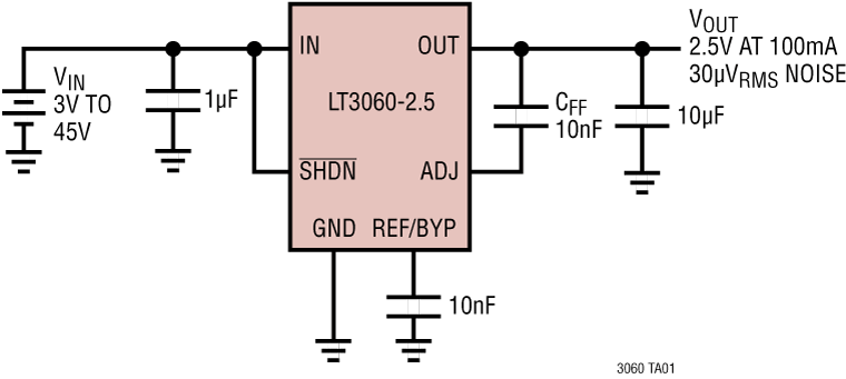
LT3060EDC-1.2#TRMPBF
Part Number : LT3060EDC-1.2#TRMPBF
Analog Devices Inc.The LT3060 series are micropower, low dropout voltage (LDO) linear regulators that operate over a 1.6V to 45V input supply range. The devices supply 100mA of output current with a typical dropout voltage of 300mV. A single external capacitor provides programmable low noise reference performance and output soft-start functionality. The LT3060’s quiescent current is merely 40μA and provides fast transient response with a minimum 2.2μF output capacitor. In shutdown, quiescent current is less than 1μA and the reference soft-start capacitor is reset.The LT3060 regulators optimize stability and transient response with low ESR, ceramic output capacitors. The regulators do not require the addition of ESR as is common with other regulators.Internal protection circuitry includes reverse-battery protection, reverse-output protection, reverse-current protection, current limit with foldback and thermal shutdown. The LT3060 series are available in fixed output voltages of 1.2V, 1.5V, 1.8V, 2.5V, 3.3V, 5V and 15V, and as an adjustable voltage regulator with an output voltage range from the 600mV reference to 44.5V. The LT3060 regulators are offered in the thermally enhanced 8-lead TSOT-23 and 8-lead (2mm × 2mm × 0.75mm) DFN packages.APPLICATIONS Battery-Powered Systems Automotive Power Supplies Industrial Power Supplies Avionic Power Supplies Portable Instruments

LT3688IFE#PBF
Part Number : LT3688IFE#PBF
Analog Devices Inc.The LT3688 is an adjustable frequency (350kHz to 2.2MHz) dual monolithic step-down switching regulator with two power-on reset timers and a watchdog timer. The regulator operates off inputs up to 36V. Low ripple Burst Mode® operation maintains high efficiency at low output current while keeping output ripple below 25mV in a typical application, with input quiescent current of just 115μA. Shutdown circuitry reduces input supply current to less than 1μA while EN/UVLO is pulled low. The reset and watchdog timeout periods are both adjustable using external capacitors. Tight accuracy specifications and glitch immunity ensure reliable reset operation without false triggering. The open collector RST pins will pull down if the monitored output voltage drops 10% below the programmed value. The LT3688 watchdog timer monitors for watchdog falling edges grouped too close together or too far apart. The LT3688 is available in 24-Pin TSSOP and 4mm × 4mm QFN packages, each with an exposed pad for low thermal resistance.Applications Automotive Electronic Control Units Industrial Power Supplies High-Reliability μProcessor Systems


