MAX7322ATE+
Part Number : MAX7322ATE+
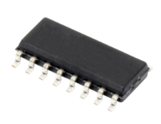
Analog Devices Inc.The MAX7322 2-wire serial-interfaced peripheral featuresfour push-pull outputs and four input ports with selectableinternal pullups. Input ports are overvoltage protected to+6V and feature transition detection with interrupt output.The four input ports are continuously monitored for statechanges (transition detection). The interrupt is latched,allowing detection of transient changes. Any combinationof inputs can be selected using the interrupt mask toassert the open-drain active-low INT output. When the MAX7322 issubsequently accessed through the serial interface, anypending interrupt is cleared.The four push-pull outputs are rated to sink 20mA, andare capable of driving LEDs.The active-low RST input clears the serial interface, terminating anyI²C communication to or from the MAX7322.The MAX7322 uses two address inputs with four-levellogic to allow 16 I²C slave addresses. The slave addressalso sets the power-up default logic state for the four outputports, and enables or disables internal 40kΩ pullups for the input ports.The MAX7322 is one device in a family of pin-compatibleport expanders with a choice of input ports, open-drainI/O ports, and push-pull output ports (see Table 1 in the full data sheet).The MAX7322 is available in 16-pin QSOP and TQFNpackages, and is specified over the -40°C to +125°Cautomotive temperature range.ApplicationsCell PhonesNotebooksSAN/NASSatellite RadioServers
MAX7324ATG+T
Part Number : MAX7324ATG+T
Analog Devices Inc.The MAX7324 2-wire serial-interfaced peripheral features16 I/O ports that are divided into eight push-pulloutputs and eight inputs. Each input features selectableinternal pullups, overvoltage protection to +6V, andtransition detection with an interrupt output.All input ports are continuously monitored for statechanges (transition detection). The interrupt is latched,allowing detection of transient changes. Any combinationof inputs can be selected using the interrupt maskto assert the active-low INT output. When the MAX7324 is subsequentlyaccessed through the serial interface, anypending interrupt is cleared.The push-pull outputs are rated to sink 20mA and arecapable of driving LEDs. The active-low RST input clears the serialinterface, terminating any I²C communication to or fromthe MAX7324.The MAX7324 uses two address inputs with four-levellogic to allow 16 I²C slave addresses. The slaveaddress also enables or disables internal 40kΩ pullups in groups of four ports.The MAX7324 is one device in a family of pin-compatibleport expanders with a choice of input ports, open-drainI/O ports, and push-pull output ports (see Table 1 in the full data sheet).The MAX7324 is available in 24-pin QSOP and TQFNpackages, and is specified over the -40°C to +125°Cautomotive temperature range.ApplicationsCell PhonesNotebooksSAN/NASSatellite RadioServers
MAX7325AEG+T
Part Number : MAX7325AEG+T
Analog Devices Inc.The MAX7325 2-wire serial-interfaced peripheral features 16 I/O ports. Ports are divided into eight push-pull outputs and eight I/Os with selectable internal pullups and transition detection. Eight ports are push-pull outputs and eight I/Os may be used as a logic input or an open-drain output. Ports are overvoltage protected to +6V.All I/O ports configured as inputs are continuously monitored for state changes (transition detection). State changes are indicated by the active-low INT output. The interrupt is latched, allowing detection of transient changes. When the MAX7325 is subsequently accessed through the serial interface, any pending interrupt is cleared. The open-drain outputs are rated to sink 20mA, and are capable of driving LEDs. The active-low RST input clears the serial interface, terminating any I2C communication to or from the MAX7325.The MAX7325 uses two address inputs with four-level logic to allow 16 I2C slave addresses. The slave address also determines the power-up logic state for the I/O ports, and enables or disables internal 40kΩ pullups in groups of four ports.The MAX7325 is one device in a family of pin-compatible port expanders with a choice of input ports, open-drain I/O ports, and push-pull output ports (see Table 1 of the full data sheet).The MAX7325 is available in 24-pin QSOP and TQFN packages and is specified over the -40°C to +125°C automotive temperature range.ApplicationsAutomotiveCell PhonesNotebooksSAN/NASSatellite RadioServers
MAX7325ATG+T
Part Number : MAX7325ATG+T
Analog Devices Inc.The MAX7325 2-wire serial-interfaced peripheral features 16 I/O ports. Ports are divided into eight push-pull outputs and eight I/Os with selectable internal pullups and transition detection. Eight ports are push-pull outputs and eight I/Os may be used as a logic input or an open-drain output. Ports are overvoltage protected to +6V.All I/O ports configured as inputs are continuously monitored for state changes (transition detection). State changes are indicated by the active-low INT output. The interrupt is latched, allowing detection of transient changes. When the MAX7325 is subsequently accessed through the serial interface, any pending interrupt is cleared. The open-drain outputs are rated to sink 20mA, and are capable of driving LEDs. The active-low RST input clears the serial interface, terminating any I2C communication to or from the MAX7325.The MAX7325 uses two address inputs with four-level logic to allow 16 I2C slave addresses. The slave address also determines the power-up logic state for the I/O ports, and enables or disables internal 40kΩ pullups in groups of four ports.The MAX7325 is one device in a family of pin-compatible port expanders with a choice of input ports, open-drain I/O ports, and push-pull output ports (see Table 1 of the full data sheet).The MAX7325 is available in 24-pin QSOP and TQFN packages and is specified over the -40°C to +125°C automotive temperature range.ApplicationsAutomotiveCell PhonesNotebooksSAN/NASSatellite RadioServers
MAX9247ECM+T
Part Number : MAX9247ECM+T
Analog Devices Inc.The MAX9247 digital video parallel-to-serial converter serializes 27 bits of parallel data into a serial-data stream. Eighteen bits of video data and 9 bits of control data are encoded and multiplexed onto the serial interface, reducing the serial-data rate. The data-enable input determines when the video or control data is serialized.The MAX9247 pairs with the MAX9248/MAX9250 deserializers to form a complete digital video serial link. Interconnect can be controlled-impedance PCB traces or twisted-pair cable. Proprietary data encoding reduces EMI and provides DC balance. DC balance allows AC-coupling, providing isolation between the transmitting and receiving ends of the interface. The LVDS output is internally terminated with 100Ω. For operating frequencies less than 35MHz, the MAX9247 can also pair with the MAX9218 deserializer.ESD tolerance is specified for ISO 10605 with ±10kV Contact Discharge and ±30kV Air-Gap Discharge.The MAX9247 operates from a +3.3V core supply and features a separate input supply for interfacing to 1.8V to 3.3V logic levels. This device is available in a 48-lead LQFP package and is specified from -40°C to +85°C or -40°C to +105°C.ApplicationsIn-Vehicle Entertainment SystemsLCDsNavigation System DisplaysVideo Cameras
MAX9250ECM+
Part Number : MAX9250ECM+
Analog Devices Inc.The MAX9248/MAX9250 digital video serial-to-parallel converters deserialize a total of 27 bits during data and control phases. In the data phase, the LVDS serial input is converted to 18 bits of parallel video data and in the control phase, the input is converted to 9 bits of parallel control data. The separate video and control phases take advantage of video timing to reduce the serial-data rate. The MAX9248/MAX9250 pair with the MAX9247 serializer to form a complete digital video transmission system. For operating frequencies less than 35MHz, the MAX9248/MAX9250 can also pair with the MAX9217 serializer.The MAX9248 features spread-spectrum capability, allowing output data and clock to spread over a specified frequency range to reduce EMI. The data and clock outputs are programmable for a spectrum spread of ±4% or ±2%. The MAX9250 features output enable input control to allow data busing.Proprietary data decoding reduces EMI and provides DC balance. The DC balance allows AC-coupling, providing isolation between the transmitting and receiving ends of the interface. The MAX9248/MAX9250 feature a selectable rising or falling output latch edge. ESD tolerance is specified for ISO 10605 with ±10kV Contact Discharge and ±30kV Air-Gap Discharge.The MAX9248/MAX9250 operate from a +3.3V ±10% core supply and feature a separate output supply for interfacing to 1.8V to 3.3V logic-level inputs. These devices are available in a 48-lead LQFP package and are specified from -40°C to +85°C or -40°C to +105°C.ApplicationsIn-Vehicle Entertainment SystemsLCD DisplaysNavigation System DisplaysVideo Cameras
MAX9250GCM+T
Part Number : MAX9250GCM+T
Analog Devices Inc.The MAX9248/MAX9250 digital video serial-to-parallel converters deserialize a total of 27 bits during data and control phases. In the data phase, the LVDS serial input is converted to 18 bits of parallel video data and in the control phase, the input is converted to 9 bits of parallel control data. The separate video and control phases take advantage of video timing to reduce the serial-data rate. The MAX9248/MAX9250 pair with the MAX9247 serializer to form a complete digital video transmission system. For operating frequencies less than 35MHz, the MAX9248/MAX9250 can also pair with the MAX9217 serializer.The MAX9248 features spread-spectrum capability, allowing output data and clock to spread over a specified frequency range to reduce EMI. The data and clock outputs are programmable for a spectrum spread of ±4% or ±2%. The MAX9250 features output enable input control to allow data busing.Proprietary data decoding reduces EMI and provides DC balance. The DC balance allows AC-coupling, providing isolation between the transmitting and receiving ends of the interface. The MAX9248/MAX9250 feature a selectable rising or falling output latch edge. ESD tolerance is specified for ISO 10605 with ±10kV Contact Discharge and ±30kV Air-Gap Discharge.The MAX9248/MAX9250 operate from a +3.3V ±10% core supply and feature a separate output supply for interfacing to 1.8V to 3.3V logic-level inputs. These devices are available in a 48-lead LQFP package and are specified from -40°C to +85°C or -40°C to +105°C.ApplicationsIn-Vehicle Entertainment SystemsLCD DisplaysNavigation System DisplaysVideo Cameras
DS1881E-050+T&R
Part Number : DS1881E-050+T&R
Analog Devices Inc.The DS1881 is a dual, nonvolatile (NV) digital potentiometer designed to operate in audio systems that require 5V signal levels. The potentiometer settings can be stored in EEPROM so that they are retained when the power is cycled. The DS1881 has separate supplies for the potentiometers (VCC) and the communication circuitry (VDD). For clickless/popless operation, a zero-crossing detector allows the wiper position to change when there is no voltage across the potentiometer. The device is also designed to minimize crosstalk, and the two digital potentiometers provide 0.5dB channel-to-channel matching to prevent volume differences between channels. Total harmonic distortion (THD) is also minimal as long as the wiper drives a high-impedance load.Two attenuation configuration options provide optimum flexibility for the specific application. Configuration Option 1 provides 63 logarithmic tapered steps (0dB to -62dB, 1dB/step) plus a mute setting. Configuration Option 2 has 32 logarithmic steps plus mute and provides software compatibility with the DS1808. When Configuration Option 2 is used in combination with the 16-pin SO package, the DS1881 is both software and pin compatible with the DS1808 in 5V applications.ApplicationsCar StereoConsumer Audio/VideoNotebook and PC AudioPortable Audio Equipment
DS2704G+T&R
Part Number : DS2704G+T&R
Analog Devices Inc.The DS2704 provides 1280 bits of EEPROM datastorage and a Secure Hash Algorithm (SHA) engine.The Dallas 1-Wire® interface enables serialcommunication on a single battery contact and the64-bit unique serial number allows multidropnetworking and identification of individual devices.The 1280-bit memory is organized as 5 pages of 32bytes each and supports storage of battery cellcharacteristics, charging voltage, current, andtemperature parameters, as well as battery packmanufacturing data. The EEPROM pages are incircuit rewritable and can be individually locked towrite protect data.The DS2704 employs the Secure Hash Algorithm(SHA-1) specified in the Federal Informationpublication 180-1 and 180-2, and ISO/IEC 10118-3.SHA-1 provides a robust cryptographic solution toensure battery packs or other peripherals have beenmanufactured by authorized sources. The DS2704processes a host transmitted challenge and the 64-bit secret key stored on chip to produce a 160-bitresponse for transmission back to the host. Thesecret key is never transmitted between the batteryand the host.Applications2.5G/3G Wireless HandsetsDigital Still and Video CamerasHandheld or Notebook Computers and TerminalsPDAs
DS4305R+T&R
Part Number : DS4305R+T&R
Analog Devices Inc.The DS4305 is a nonvolatile (NV) electronically programmable voltage reference. The reference voltage is programmed in-circuit during factory calibration/programming. Programming the reference voltage, VOUT, is as simple as applying the desired voltage on VIN and toggling the adjust pin (active-low ADJ) to lock the VOUT voltage level indefinitely, even if the device is power cycled. The DS4305 replaces current cumbersome factory adjustment arrangements with a low-cost solution that can be adjusted using automated techniques. In addition, the DS4305 has the ability to be readjusted after the unit has been fully assembled and tested. This results in a much more flexible manufacturing arrangement, lower inventory costs, and a quicker time-to-market.ApplicationsBias AdjustingFactory-Calibrated EquipmentOffset NullingPower AmpsPower Supply CalibrationPressure BridgesThreshold Setting
LTC3525ISC6-5#TRPBF
Part Number : LTC3525ISC6-5#TRPBF
Analog Devices Inc.The LTC3525-3/LTC3525-3.3/LTC3525-5 are high efficiency synchronous step-up DC/DC converters with output disconnect that can start up with an input as low as 0.85V. They offer a compact, high efficiency alternative to charge pumps in single cell or dual cell alkaline or Li-Ion applications. Only three small external components are required. The LTC3525 is offered in fixed output voltages of 3V, 3.3V or 5V.The device includes a 0.5Ω N-channel MOSFET switch and a 0.8Ω P-channel synchronous rectifier. Peak switch current ranges from 150mA to 400mA, depending on load, providing enhanced efficiency. Quiescent current is an ultralow 7μA, maximizing battery life in portable applications.Other features include
LTC3726EGN#PBF
Part Number : LTC3726EGN#PBF
Analog Devices Inc.The LTC3726 is a secondary-side controller for synchronous forward converters. When used in conjunction with the LTC3705/LTC3725 gate driver and primary-side controllers, the part creates a complete isolated power supply that combines the simplicity of OPTI-LOOP® compensation with the speed of secondary-side control.The LTC3726 has been designed to simplify the design of highly efficient, secondary-side forward converters. Working in concert with the LTC3705 or LTC 3725, the LTC3726 forms a robust, self-starting converter that eliminates the need for the separate bias regulator that is commonly used in secondary-side control applications. In addition, a proprietary scheme is used to multiplex gate drive signals and DC bias power across the isolation barrier through a single, tiny pulse transformer.The LTC3726 is available in a 16-lead SSOP package.Applications Isolated 48V Telecommunication Systems Internet Servers and Routers Distributed Power Step-Down Converters Automotive and Heavy Equipment
MAX13020ASA+
Part Number : MAX13020ASA+
Analog Devices Inc.The MAX13020/MAX13021 ±60V fault-protected low-power local interconnect network (LIN) transceivers are ideal for use in automotive network applications where high reliability is required. The devices provide the interface between the LIN master/slave protocol controller, and the physical bus described in the LIN 2.0 specification package and SAE J2602 specification. The devices are intended for in-vehicle subnetworks with a single master and multiple slaves.The extended fault-protected voltage range of ±60V on the LIN bus line allows for use in +12V, +24V, and +42V automotive applications. The devices allow communication up to 20kbaud, and include slew-rate limited transmitters for enhanced electromagnetic emissions (EME) performance. The devices feature a low-power 4µA sleep mode and provide wake-up source detection.The MAX13020 is a pin-to-pin replacement and is functionally compatible with the Philips TJA1020. The MAX13021 includes enhanced bus dominant clamping fault management for reduced quiescent current during LIN bus shorts to GND. The MAX13020/MAX13021 are available in the 8-pin SO package, and operate over the -40°C to +125°C automotive temperature range.Applications+12V and +42V Automotive+24V Heavy Truck and Bus
MAX15013BASA+
Part Number : MAX15013BASA+
Analog Devices Inc.The MAX15012/MAX15013 high-frequency, 175V half-bridge, n-channel MOSFET drivers drive high- and low-side MOSFETs in high-voltage applications. These drivers are independently controlled and their 35ns typical propagation delay, from input to output, are matched to within 2ns (typ). The high-voltage operation with very low and matched propagation delay between drivers, and high source/sink current capabilities make these devices suitable for the high-power, high-frequency telecom power converters. A reliable on-chip bootstrap diode connected between VDD and BST eliminates the need for an external discrete diode.The MAX15012A/C and MAX15013A/C offer both noninverting drivers (see the Selector Guide of the full data sheet). The MAX15012B/D and MAX15013B/D offer a noninverting high-side driver and an inverting low-side driver. The MAX15012A/B/C/D feature CMOS (VDD/2) logic inputs. The MAX15013A/B/C/D feature TTL logic inputs. The drivers are available in the industry-standard 8-pin SO footprint and pin configuration and a thermally enhanced 8-pin SO package. All devices operate over the -40°C to +125°C automotive temperature range.ApplicationsActive-Clamp Forward ConvertersFull-Bridge ConvertersMotor ControlPower-Supply ModulesTelecom Half-Bridge Power SuppliesTwo-Switch Forward Converters
MAX15013BASA+T
Part Number : MAX15013BASA+T
Analog Devices Inc.The MAX15012/MAX15013 high-frequency, 175V half-bridge, n-channel MOSFET drivers drive high- and low-side MOSFETs in high-voltage applications. These drivers are independently controlled and their 35ns typical propagation delay, from input to output, are matched to within 2ns (typ). The high-voltage operation with very low and matched propagation delay between drivers, and high source/sink current capabilities make these devices suitable for the high-power, high-frequency telecom power converters. A reliable on-chip bootstrap diode connected between VDD and BST eliminates the need for an external discrete diode.The MAX15012A/C and MAX15013A/C offer both noninverting drivers (see the Selector Guide of the full data sheet). The MAX15012B/D and MAX15013B/D offer a noninverting high-side driver and an inverting low-side driver. The MAX15012A/B/C/D feature CMOS (VDD/2) logic inputs. The MAX15013A/B/C/D feature TTL logic inputs. The drivers are available in the industry-standard 8-pin SO footprint and pin configuration and a thermally enhanced 8-pin SO package. All devices operate over the -40°C to +125°C automotive temperature range.ApplicationsActive-Clamp Forward ConvertersFull-Bridge ConvertersMotor ControlPower-Supply ModulesTelecom Half-Bridge Power SuppliesTwo-Switch Forward Converters
MAX16002ATC+
Part Number : MAX16002ATC+
Analog Devices Inc.The MAX16000–MAX16007 are low-voltage, quad-/hex-/octal-voltage µP supervisors in small TQFN and TSSOP packages. These devices provide supervisory functions for complex multivoltage systems. The MAX16000/MAX16001/MAX16002 monitor four voltages, the MAX16003/MAX16004/MAX16005 monitor six voltages, and the MAX16006/MAX16007 monitor eight voltages. The MAX16000/MAX16001/MAX16003/MAX16004/MAX16006 offer independent outputs for each monitored voltage. The MAX16001/MAX16002/MAX16004–MAX16007 offer a reset output that asserts whenever any of the monitored voltages fall below their respective thresholds or the manual reset input is asserted. The reset output remains asserted for the reset timeout after all voltages are above their respective thresholds and the manual reset input is deasserted. The minimum reset timeout is internally set to 140ms or can be adjusted with an external capacitor.All open-drain outputs have internal 30µA pullups that eliminate the need for external pullup resistors. However, each output can be driven with an external voltage up to 5.5V. Other features offered include a manual reset input, a tolerance pin for selecting 5% or 10% input thresholds, and a margin enable function for deasserting the outputs during margin testing.The MAX16001/MAX16002/MAX16004–MAX16007 offer a watchdog timer that asserts active-low RESET or an independent watchdog output (MAX16005) when the watchdog timeout period (1.6s typ) is exceeded. The watchdog timer can be disabled by leaving the input open.These devices are offered in 12-, 16-, 20-, and 24-lead TQFN and 16-lead TSSOP packages. These are fully specified from -40°C to +125°C.ApplicationsMultivoltage ASICsNetworking/Telecommunication EquipmentServersStorage Equipment
MAX16029TG+
Part Number : MAX16029TG+
Analog Devices Inc.The MAX16025–MAX16030 are dual-/triple-/quad-voltagemonitors and sequencers that are offered in asmall TQFN package. These devices offer enormousdesign flexibility as they allow fixed and adjustablethresholds to be selected through logic inputs and providesequence timing through small external capacitors.These versatile devices are ideal for use in a widevariety of multivoltage applications.As the voltage at each monitored input exceeds itsrespective threshold, its corresponding output goeshigh after a propagation delay or a capacitor-set timedelay. When a voltage falls below its threshold, itsrespective output goes low after a propagation delay.Each detector circuit also includes its own enable input,allowing the power-good outputs to be shut off independently.The independent output for each detector isavailable with push-pull or open-drain configurationwith the open-drain version capable of supporting voltagesup to 28V, thereby allowing them to interface toshutdown and enable inputs of various DC-DC regulators.Each detector can operate independently as fourseparate supervisory circuits or can be daisy-chainedto provide controlled power-supply sequencing.The MAX16025–MAX16030 also include a reset functionthat deasserts only after all of the independentlymonitored voltages exceed their threshold. The resettimeout is internally fixed or can be adjusted externally.These devices are offered in a 4mm x 4mm TQFNpackage and are fully specified from -40°C to +125°C.ApplicationsDC-DC SuppliesMultivoltage SystemsNetworking/Telecommunication EquipmentServers/WorkstationsStorage Systems
MAX16803ATE+
Part Number : MAX16803ATE+
Analog Devices Inc.The MAX16803 current regulator operates from a 6.5V to 40V input-voltage range and delivers up to a total of 350mA to one or more strings of high-brightness LEDs (HB LEDs). The output current of the MAX16803 is adjusted by using an external current-sense resistor in series with the LEDs. A dimming input allows widerange 'pulsed' PWM operation. Wave-shaping circuitry reduces EMI. The differential current-sense input increases noise immunity. The MAX16803 is well suited for applications requiring high-voltage input and is able to withstand automotive load-dump events up to 40V. An on-board pass element minimizes external components while providing ±3.5% output-current accuracy. Additional features include a 5V regulated output and short-circuit and thermal protection.The MAX16803 is available in a thermally enhanced, 5mm x 5mm, 16-pin TQFN package and is specified over the automotive -40°C to +125°C temperature range.The MAX16836 is a newer and more cost effective product; except for different PWM dimming current slew rates, it provides the same performance and is pin-to-pin compatible with the MAX16803.ApplicationsAutomotive Exterior: Rear Combination Lights (RCL)Automotive Interior: Map, Courtesy, and Cluster LightingEmergency Vehicle Warning LightsGeneral LightingNavigation and Marine IndicatorsSignage, Gasoline Canopies, Beacons
MAX3643ETG+T
Part Number : MAX3643ETG+T
Analog Devices Inc.The MAX3643 burst-mode laser driver provides bias and modulation current drive for PON burst-mode ONT applications. It is specifically designed for use with a low-cost external controller for the APC (and if desired, AMC) loop. A high-speed differential burst-enable input enables the driver to switch the laser from a dark (output off) condition to full on condition in less than 2ns.When BEN is inactive, typical modulation and bias currents are 5µA each.Laser modulation current can be set from 10mA to 85mA and bias current can be set from 1mA to 70mA using the MODSET and BIASSET inputs. A sample-and-hold circuit is provided to capture the monitor diode output during short PON bursts, if needed, and the BEN high-speed signal is mirrored on an LVCMOS output to be used by the controller operating the APC/AMC loop.The MAX3643 burst-mode laser driver is packaged in a 4mm x 4mm, 24-pin thin QFN package. It operates from -40°C to +85°C.Applications1.25Gbps IEEE EPON ONT ModulesA/B/G/XGPON ONT Modules Up to 2.5Gbps
MAX4885ETJ+
Part Number : MAX4885ETJ+
Analog Devices Inc.The MAX4885 integrates high-bandwidth analog switches and level translating buffers to implement a complete 1:2 or 2:1 multiplexer for VGA signals. The device provides switching for RGB, display data channel (DDC), and horizontal and vertical synchronization (HSYNC, VSYNC) signals. A low-noise charge pump with internal capacitors provides a boosted gate-drive voltage to improve performance of the RGB switches. In the 1:2 multiplexer mode, HSYNC/VSYNC inputs feature level-shifting buffers to support low voltage CMOS or standard TTL-compatible graphics controllers. In the 2:1 multiplexer mode, the output buffers for the HSYNC/VSYNC inputs are disabled, allowing bidirectional signaling. In both modes, DDC signals are voltage-clamped to an external voltage to provide level translation and protection. The MAX4885 features a 5µA shutdown mode and is ESD protected to ±8kV human body model (HBM) on externally routed pins.The MAX4885 is specified over the extended (-40°C to +85°C) temperature range, and is available in the 32-pin, 5mm x 5mm TQFN package.ApplicationsNotebook ComputersServers


