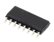
LTC2946CDE-1#PBF
Part Number : LTC2946CDE-1#PBF
Analog Devices Inc.The LTC2946 is a rail-to-rail system monitor that measures current, voltage, power, charge and energy. It features an operating range of 2.7V to 100V and includes a shunt regulator for supplies above 100V. The current measurement common mode range of 0V to 100V is independent of the input supply. A 12-bit ADC measures load current, input voltage and an auxiliary external voltage. Load current and internally calculated power are integrated over an external clock or crystal or internal oscillator time base for charge and energy. An accurate time base allows the LTC2946 to provide measurement accuracy of better than ±0.6% for charge and ±1% for power and energy. Minimum and maximum values are stored and an overrange alert with programmable thresholds minimizes the need for software polling. Data is reported via a standard I2C interface.The LTC2946 I2C interface includes separate data input and output pins for use with standard or opto-isolated I2C connections. The LTC2946-1 has an inverted data output for use with inverting opto-isolator configurations.Applications Telecom Infrastructure Industrial Equipment General Purpose Energy Measurement
LTC3106IFE#TRPBF
Part Number : LTC3106IFE#TRPBF
Analog Devices Inc.The LTC3106 is a highly integrated, ultralow voltage buck-boost DC/DC converter with automatic PowerPath management optimized for multisource, low power systems. At no load, the LTC3106 draws only 1.6μA while creating an output voltage up to 5V from either input source.If the primary power source is unavailable, the LTC3106 seamlessly switches to the backup power source. The LTC3106 is compatible with either rechargeable or primary cell batteries and can trickle charge a backup battery whenever there is an energy surplus available. Optional maximum power point control ensures power transfer is optimized between power source and load. The output voltage and backup voltage, VSTORE, are programmed digitally, reducing the required number of external components. Zero power Shelf Mode ensures that the backup battery will remain charged if left connected to the LTC3106 for an extended time.Additional features include an accurate turn-on voltage, a power good indicator for VOUT, a user selectable 100mA peak current limit setting for lower power applications, thermal shutdown as well as user selectable backup power and output voltages.Applications Wireless Sensor Networks Home or Office Building Automation Energy Harvesting Remote Sensors
LTC3118EFE#PBF
Part Number : LTC3118EFE#PBF
Analog Devices Inc.The LTC3118 is a dual-input, wide voltage range synchronous buck-boost DC/DC converter with an intelligent, integrated, low loss PowerPath control. The unique power switch architecture provides efficient operation from either input source to a programmable output voltage above, below or equal to the input. Voltage capability of up to 18V provides flexibility and voltage margin for a wide variety of applications and power sources.The LTC3118 uses a low noise, current mode architecture with a fixed 1.2MHz PWM mode frequency that minimizes the solution footprint. For high efficiency at light loads, automatic Burst Mode operation can be selected consuming only 50μA of quiescent current in sleep.System level features include ideal diode or VIN priority modes, VIN and VOUT power good indicators, accurate RUN comparators to program independent UVLO thresholds, and output disconnect in shutdown. Other features include 2μA shutdown current, short-circuit protection, soft-start, current limit and thermal overload protection.The LTC3118 is offered in thermally enhanced 24-lead 4mm × 5mm QFN and 28-lead TSSOP packages.Applications Systems with Multiple Input Sources Back Up Power Systems Wall Adapter or Li-Ion(s) Input to 5VOUT Battery or Super Capacitor Input for Reserve Power Replace Diode-OR Designs with Higher Efficiency, Flexibility and Performance
LTC3118EUFD#TRPBF
Part Number : LTC3118EUFD#TRPBF
Analog Devices Inc.The LTC3118 is a dual-input, wide voltage range synchronous buck-boost DC/DC converter with an intelligent, integrated, low loss PowerPath control. The unique power switch architecture provides efficient operation from either input source to a programmable output voltage above, below or equal to the input. Voltage capability of up to 18V provides flexibility and voltage margin for a wide variety of applications and power sources.The LTC3118 uses a low noise, current mode architecture with a fixed 1.2MHz PWM mode frequency that minimizes the solution footprint. For high efficiency at light loads, automatic Burst Mode operation can be selected consuming only 50μA of quiescent current in sleep.System level features include ideal diode or VIN priority modes, VIN and VOUT power good indicators, accurate RUN comparators to program independent UVLO thresholds, and output disconnect in shutdown. Other features include 2μA shutdown current, short-circuit protection, soft-start, current limit and thermal overload protection.The LTC3118 is offered in thermally enhanced 24-lead 4mm × 5mm QFN and 28-lead TSSOP packages.Applications Systems with Multiple Input Sources Back Up Power Systems Wall Adapter or Li-Ion(s) Input to 5VOUT Battery or Super Capacitor Input for Reserve Power Replace Diode-OR Designs with Higher Efficiency, Flexibility and Performance
LTC3265HFE#PBF
Part Number : LTC3265HFE#PBF
Analog Devices Inc.The LTC3265 is a low noise dual polarity output power supply including a boost charge pump, an inverting charge pump and two low noise positive and negative LDO post regulators. The boost charge pump powers the positive LDO post regulator while the inverting charge pump powers the negative LDO regulator. Each LDO can provide up to 50mA of output current. The LDO output voltages can be adjusted using external resistor dividers.The charge pumps employ low quiescent current Burst Mode operation or low noise constant frequency mode. During Burst Mode operation, the boost charge pump regulates its output (VOUT +) to 0.94 • 2 • VIN_P while the inverting charge pump regulates its output (VOUT –) to –0.94 • VIN_N. In Burst Mode operation the LTC3265 draws only 135μA of quiescent current with both LDOs on. In constant frequency mode, the boost and inverting charge pumps produce outputs equal to 2 • VIN_P and –VIN_N respectively and operate at a fixed 500kHz or to a programmed value between 50kHz to 500kHz using an external resistor. The LTC3265 is available in low profile 3mm × 5mm × 0.75mm 18-lead DFN and thermally enhanced 20-lead TSSOP packages.Applications Low Noise Bipolar/Inverting Supplies Industrial/Instrumentation Low Noise Bias Generators
AD4684BCPZ-RL
Part Number : AD4684BCPZ-RL
Analog Devices Inc.The AD4684/AD4685 are 16-bit, dual, simultaneous sampling, high speed, successive approximation register (SAR), analog-to-digital converters (ADCs) that operate from a 3.0 V to 3.6 V power supply and feature throughput rates of up to 1 MSPS for the AD4684 and 500 kSPS for the AD4685. The analog input types are single-ended and are sampled and converted on the falling edge of CS.The AD4684/AD4685 have an on-chip sequencer and integrated on-chip oversampling block to improve dynamic range and reduce noise at lower bandwidths. A buffered internal 2.5 V reference is included. Alternatively, an external reference up to 3.3 V can be used. The conversion process and data acquisition use standard control inputs, allowing interfacing to microprocessors or digital signal processors (DSPs). The AD4684/AD4685 is compatible with 1.8 V, 2.5 V, and 3.3 V interfaces by using the separate logic supply. The AD4684/AD4685 are available in a 16-lead, 3 mm × 3 mm lead frame chip scale package (LFCSP) with operation specified from −40°C to +125°C.PRODUCT HIGHLIGHTS 4-channel, dual simultaneous sampling ADC. Pin-compatible product family. High throughput rate: 1 MSPS (AD4684) and 500 kSPS (AD4685). Space-saving, 16-lead, 3 mm × 3 mm LFCSP. Integrated oversampling block to increase dynamic range and SNR and to reduce SCLK speed requirements. Single-ended analog inputs. Small sampling capacitor reduces amplifier drive burden. APPLICATIONS Motor control position feedback Motor control current sense Sonars Power quality Data acquisition systems Erbium doped fiber amplifier (EDFA) applications Inphase and quadrature demodulation
ADA4945-1ACPZ-R7
Part Number : ADA4945-1ACPZ-R7
Analog Devices Inc.The ADA4945-1 is a low noise, low distortion, fully differential amplifier with two selectable power modes. The device operates over a broad power supply range of 3 V to 10 V. The low dc offset, dc offset drift, and excellent dynamic performance of the ADA4945-1 makes it well suited for a variety of data acquisition and signal processing applications. The device is an ideal choice for driving high resolution, high performance successive approximation register (SAR) and Σ-Δ analog-to-digital converters (ADCs) on 4 mA of quiescent current (full power mode). The device can also be selected to operate on 1.4 mA of quiescent current (low power mode) to scale the power consumption to the desired performance necessary for an ADC drive application. The adjustable common-mode voltage allows the ADA4945-1 to match the input common-mode voltage of multiple ADCs. The internal common-mode feedback loop provides exceptional output balance, as well as suppression of even order harmonic distortion products.With the ADA4945-1, differential gain configurations are achieved with a simple external feedback network of four resistors determining the closed-loop gain of the amplifier. The ADA4945-1 is fabricated using Analog Devices, Inc., proprietary, silicon germanium (SiGe), complementary bipolar process, enabling the device to achieve low levels of distortion with an input voltage noise of only 1.8 nV/√Hz (full power mode).The ADA4945-1 is available in a RoHS-complaint, 3 mm × 3 mm, 16-lead LFCSP. The ADA4945-1 is specified to operate from −40°C to +125°C.Applications Low power Σ-Δ, PulSAR®, and SAR ADC drivers Single-ended to differential converters Differential buffers Medical imaging Process control Portable electronics
ADBMS2952WCCSZ
Part Number : ADBMS2952WCCSZ
Analog Devices Inc.ADBMS2950 and ADBMS2952 are Battery Pack Monitors for electrical and hybrid vehicles, and other current or voltage sense applications. ADBMS2950 and ADBMS2952 measure the current flowing in and out of a battery pack by sensing the voltage drop over a shunt resistor with a very low offset.ADBMS2950 and ADBMS2952 also detect Overcurrent conditions using fast Overcurrent ADCs with digital threshold comparators and communicate their results through dedicated Overcurrent alert lines with minimum delay.ADBMS2950 and ADBMS2952 feature a total of 12 internally buffered high impedance inputs for measuring voltages from external sensors or resistor dividers, enabling measurement of pack voltages, temperatures, HV-Link voltages, chassis isolation, and the supervision of the state of contactors and fuses. Six digital outputs (GPO) supporting open-drain or push-pull can be used to control high voltage transistors to disconnect external resistor dividers. Four digital general-purpose inputs/outputs (GPIO) also allow operation as an I2C or SPI controller interface to address an external EEPROM or other serial peripherals.The built-in serial interface of ADBMS2950 can be configured for SPI or isolated isoSPI communication to the host. An additional isoSPI port allows to connect a daisy chain of ADBMS2950 devices; optionally extended with ADBMS6830 or ADBMS6832 (ADBMS683x) Cell Monitors. The ADBMS2952 supports SPI communication only.APPLICATIONS Electric and Hybrid Electric Vehicles Backup Battery Systems Grid Energy Storage
LTC9101AUF-2#PBF
Part Number : LTC9101AUF-2#PBF
Analog Devices Inc.The LTC9101-2 chipset is a 12/24-port power sourcing equipment (PSE) controller designed for use in IEEE 802.3bt Type 3 and 4 compliant Power over Ethernet (PoE) systems. The LTC9101-2/LTC9102 is designed to power compliant 802.3af, 802.3at, and 802.3bt PDs. The LTC9101-2/LTC9102 chipset delivers lowest-in-industry heat dissipation by utilizing low RDS(ON) external MOSFETs and 0.1Ω sense resistance per power channel. A transformer-isolated communication protocol replaces expensive opto-couplers and complex isolated 3.3V supply, resulting in significant BOM cost savings.Advanced power management features include per-port 14‑bit current/voltage monitoring, programmable power limits, and versatile fast shut down of preselected ports. An advanced power management host software layer is available. PD detection uses a proprietary multipoint detection mechanism ensuring excellent immunity from false PD identification. Autoclass and 5-event physical classification are supported. The LTC9101-2/LTC9102 includes an I2C serial interface operable up to 1MHz. The LTC9101-2/LTC9102 is pin or I2C programmable to negotiate PD delivered power up to 71.3W.APPLICATIONS PoE PSE Switches/Routers and Midspans
LTC9101AUF-3#PBF
Part Number : LTC9101AUF-3#PBF
Analog Devices Inc.The LTC9101-3/LTC9103 chipset is a 8/16-port power sourcing equipment (PSE) controller and power manager designed for use in IEEE 802.3at compliant Power over Ethernet (PoE) systems. The LTC9101-3 manages a user-defined system-level power budget across all ports. Port power is automatically assigned based on system power availability, initial physical classification and after power up, port dynamic power consumption.The LTC9101-3 prioritizes port power by port number (port 1 is highest priority) and automatically removes power from lower priority ports to accommodate higher priority ports.The LTC9101-3 features an interface to control an external serial LED driver. LED indications include Port On, Port Off, Port Power Denied, and Port Fault states. A Supply Overload LED indicates system power usage is near power limit or a port is being denied power.The LTC9101-3 operates without a host present. Configuration is accomplished by pin settings and I2C-based flash programming.The LTC9101-3 autonomously performs compliant 802.3at detection, classification power up, power on, and fault management.APPLICATIONS Small Business PoE PSE Switches/Routers
MAX14432FASE+T
Part Number : MAX14432FASE+T
Analog Devices Inc.The MAX14430–MAX14432 are fast, low power, 4-channel, digital galvanic isolators using Maxim’s proprietary process technology. These devices transfer digital signals between circuits with different power domains while using as little as 0.58mW per channel at 1Mbps with a 1.8V supply. The MAX14430–MAX14432 have an isolation rating of 3kVRMS (QSOP package) or 3.75kVRMS (narrow SOIC package) for 60 seconds. For applications requiring 5kVRMS of isolation, see the MAX14434-MAX14436.The MAX14430–MAX14432 family offers all three possible unidirectional channel configurations to accommodate any 4-channel design, including SPI, RS-232, RS-485, and digital I/O applications. Output enable for the A side of the MAX14431R/S/U/V is active-low, making them ideal for isolating a port on a shared SPI bus since the active-low CS signal can directly enable the MISO signal on the isolator. All other devices in the family have the traditional active-high enable.Devices are available with a maximum data rate of either 25Mbps or 200Mbps and with outputs that are either default-high or default-low. The default is the state the output assumes when the input is either not powered or is open-circuit. See the Ordering Information and Product Selector Guide for suffixes associated with each option. Independent 1.71V to 5.5V supplies on each side of the isolator also make the devices suitable for use as level translators.The MAX14430–MAX14432 are available either in a 16-pin narrow-body SOIC package with 4mm of creepage and clearance, or in a smaller 16-pin QSOP package with 4mm of creepage and clearance. The SOIC package material has a minimum comparative tracking index (CTI) of 600, which gives it a group I rating in creepage table. The QSOP package material has a minimum CTI of 400, which gives it a group II rating in creepage table. All devices are rated for operation at ambient temperatures of -40°C to +125°C.ApplicationsBattery ManagementFieldbus Communications for Industrial AutomationIsolated RS-485/RS-422, CANIsolated SPI InterfaceMedical Systems
MAX15093AGWL+T
Part Number : MAX15093AGWL+T
Analog Devices Inc.The MAX15093/MAX15093A ICs are integrated solutions for hot-swap applications requiring the safe insertion and removal of circuit-line cards from a live backplane. The devices integrate a hot-swap controller, 3.8mΩ power MOSFET, and an electronic circuit-breaker protection in a single package.The devices integrate an accurate current-sense circuitry and provide 160µA/A of proportional output current. The devices are designed for protection of 2.7V to 18V supply voltages.These devices implement a foldback current limit during startup to control inrush current lowering di/dt and keep the MOSFET operating under safe operating area (SOA)conditions. After the startup cycle is complete, on-chip comparators provide VariableSpeed/BiLevel™ protection against short-circuit and overcurrent faults, and immunity against system noise and load transients. The load is disconnected in the event of a fault condition. The devices are factory calibrated to deliver accurate overcurrent protection with ±10% accuracy. During a fault condition, the MAX15093 latches off, while the MAX15093A enters autoretry mode.The devices feature an IN-to-OUT short-circuit detection before startup. The devices provide a power-MOSFET GATE pin to program the slew rate during startup by adding an external capacitor. The devices have overvoltage/undervoltage input pins that can detect an overvoltage/undervoltage fault and disconnect the IN from the OUT. Additional features include internal overtemperatureprotection, power-good output, and fault-indicator output.The MAX15093/MAX15093A ICs are available in a 40-bump, 2.57mm x 4.03mm, power wafer-level package (WLP) and are rated over the -40°C to +105°C extended temperature range.ApplicationsDisk Drive PowerIndustrialRAID SystemsServer I/O CardsStorage Bridge Bay
MAX16160NCAB+T
Part Number : MAX16160NCAB+T
Analog Devices Inc.The MAX16160 precision, four-channel supervisory circuit is designed to maintain system integrity in multi-supply systems.The device monitors its own power supply voltage in addition to three other system supply voltages and asserts the reset output whenever any supply voltage falls below its reset threshold. After all of the supply voltages rise above their reset thresholds, the reset output remains asserted for the reset timeout period, and then de-asserts.During power-up, and before all of the input voltages exceed their trip thresholds, the reset output asserts low if any of the monitored inputs is greater than 1V. The open-drain output has a weak 18μA (typ) pullup to IN2/VCC, eliminating the need for external pullup resistors.The MAX16160 offers a wide range of threshold options. Input thresholds may be fixed or adjustable. Fixed reset voltage thresholds for IN1, IN3, IN4 are available from 0.5V to 5V in approximately 20mV increments. Reset voltage thresholds for IN2/VCC are available from 1.76V to 5V in approximately 20mV increments.The MAX16160 operates over the -40°C to +125°C temperature and is available in a small, 6-bump WLP and 6-pin SOT23 package.ApplicationsData Storage EquipmentDesktop and Notebook ComputersHigh-End PrintersIndustrial EquipmentNetworking EquipmentServers/WorkstationsSet-Top BoxesTelecommunications
MAX16162NGK190+T
Part Number : MAX16162NGK190+T
Analog Devices Inc.The MAX16161/MAX16162 are ultra-low current, singlechannelsupervisory ICs. The devices monitor the powersupply voltage and assert a reset when the input voltagefalls below the reset threshold. After the monitoring voltagerises above the factory-set threshold voltage (VTH),the reset output remains asserted for the reset timeoutperiod and then deasserts, allowing the target microcontrolleror microprocessor to leave the reset state and beginoperating.Unlike conventional supervisors, which are unable to controlthe reset output state when VCC is very low, theMAX16161/MAX16162 reset output is guaranteed to remainasserted until after a valid VCC is achieved. Thisis especially important to avoid low-voltage cores leavingthe reset state during power-up or power-down. This alsoimproves performance when using the MAX16161/MAX16162 as simple power supply sequencers, becausethe devices will never cause a transient enable of a downstreampower supply due to output glitches.The MAX16161 features a manual reset (MR) input thatasserts a reset when it receives an appropriate input signal,which may be either active-low or active-high, dependingon the option. The MAX16162 has no MR input.Instead, it has separate VCC and VIN pins, allowingthreshold voltages as low as 0.6V. The reset output is active-low open-drain, and the MAX16161/MAX16162 offermultiple available reset timeout period options.The MAX16161/MAX16162 are specified over the -40°Cto +125°C temperature range and are available in tiny,1.06mm x 0.73mm, 4-bump WLP and 4-pin SOT23 packages. The MAX16162 is also available in a 5-pin SOT23 package.Applicationse-Readers/TabletsLow-Voltage Microcontrollers and MicroprocessorsPortable/Battery-Powered EquipmentSmart PhonesWearable/Portable Accessories
MAX16165ATPH+T
Part Number : MAX16165ATPH+T
Analog Devices Inc.The MAX16165/MAX16166 monitor up to five voltages and sequence up to four voltages. These devices provide an adjustable delay as each supply is turned on as well as monitor each power-supply voltage, including the input voltage VDD.The MAX16165/MAX16166 operate from a supply range of 2.7V to 16V and have an internal regulator output (ABP), power internal circuits, and supply more than 1mA additional current to any external circuitry.The sequencing is enabled by two inputs, ON and active-low OFF. A rising edge on the ON input initiates power-on sequencing of the channels whereas a falling edge on active-low OFF input initiates power-off sequencing. During the power-on sequencing, when all of the voltages reach their final values, a sequencing done output DONE asserts high followed by a Power-OK (POK) output after the reset delay timer has expired, allowing the microcontroller (µC) to operate. If any voltage falls below its threshold, the reset output asserts and all voltage supplies are turned off. When the sequencer initiates a power-off sequencing, the MAX16165/MAX16166 can reverse sequence the outputs.Output options available are open-drain (MAX16165) and push-pull (MAX16166). The MAX16165/MAX16166 can be daisy-chained unlimited amount to time to control any number of voltages in a system.The MAX16165/MAX16166 feature a bidirectional active-low FAULT input/output, which asserts low during any fault condition. Active-low FAULT stays low as long as an undervoltage event is present at UVSET Input and it is a one-shot output during all other active-low FAULT conditions. An external signal pulling active-low FAULT low disables all outputs immediately. The MAX16165/MAX16166 are available in a 1.63mm x 2.03mm, 20-bump Wafer-Level Package (WLP) and a 4mm x 4mm, 20L TQFN package. The device is fully specified over the -40°C to +125°C operating temperature range.ApplicationsFPGA/ASIC Power Supply SequencingIndustrial Sensors and Motor ControlsLatch-Up Prevention and Inrush Current Protection in Multi-Supply SystemsNetworking EquipmentServers and Security CamerasTest Equipment
MAX16926GTP/V+
Part Number : MAX16926GTP/V+
Analog Devices Inc.The MAX16926 is a 4-channel power-management IC designed to accommodate the main rails used in modern automotive TFT displays. The MAX16926 and the MAX20069 TFT power supply and LED backlight driver combine to provide a two-chip solution to automotive display power supply requirements.The MAX16926 integrates a high-voltage buck converter that transforms battery voltages into a 3.3V intermediate rail. In addition, a high-voltage, always-on, low-quiescent-current linear regulator supplies power at 3.3V. The low-voltage section consists of a fully-integrated DC/DC converter and an LDO running off the intermediate rail. The low-voltage DC/DC converter provides 1.1V, while the LDO produces 1.8V. In addition, an integrated watchdog timer guards against runaway code.A single START control pin initiates the start-up sequence, thereby simplifying device control. The MAX16926's external pMOSFET control block allows battery voltage to be switched to a downstream device, such as a backlight boost converter. The MAX16926 is available in a TQFN package and operates in the -40°C to 105°C temperature range.ApplicationsInfotainment DisplaysCentral Information DisplaysInstrument Clusters
MAX17301G+
Part Number : MAX17301G+
Analog Devices Inc.The MAX17300–MAX17303/MAX17310–MAX17313 is a 24μA IQ stand-alone pack-side fuel gauge IC with protector and optional SHA-256 authentication for 1-cell lithium-ion/polymer batteries.The IC monitors the voltage, current, temperature, and state of the battery to provide against over/undervoltage, overcurrent, short-circuit, over/undertemperature and overcharge conditions protection using external high-side N-FETs, and provides charging prescription to ensure that the lithium-ion/polymer battery operates under safe conditions prolonging the life of the battery.To prevent battery pack cloning, the IC integrates SHA-256 authentication with a 160-bit secret key. Each IC incorporates a unique 64-bit ID.The fuel gauge uses ModelGauge m5 algorithm that combines the short-term accuracy and linearity of a coulomb counter with the long-term stability of a voltage-based fuel gauge to provide industry-leading fuel-gauge accuracy.The IC automatically compensates for cell aging, temperature, and discharge rate, and provides accurate state-of-charge (SOC) in milliampere-hours (mAh) or percentage (%) over a wide range of operating conditions.Dynamic power functionality provides the instantaneous maximum battery output power which can be delivered to the system without violating the minimum system input voltage.A Maxim 1-Wire® or 2-wire I2C interface provides access to data and control registers. The IC is available in a lead-free, 3mm x 3mm 14-pin TDFN and 1.7mm x 2.5mm 15-bump 0.5mm pitch WLP packages.ApplicationsSmartphones, Tablets, and 2-in-1 LaptopsSmartwatches and WearablesMedical Devices, Health and Fitness MonitorsDigital Still, Video, and Action CamerasHandheld Computers and TerminalsHandheld RadiosHome and Building Automation, SensorsSmart Batteries
MAX17643ATC+T
Part Number : MAX17643ATC+T
Analog Devices Inc.The Himalaya series of voltage regulator ICs, power modules,and chargers enable cooler, smaller, and simplerpower-supply solutions. The MAX17643 high-efficiency,high-voltage, Himalaya synchronous step-down DC-DCconverter with integrated MOSFETs operates over a 4.5Vto 60V input. The converter can deliver up to 2A and generatesoutput voltages from 0.9V up to (0.9 x VIN)V. Thefeedback (FB) voltage is accurate to within ±.4% over-40°C to +125°C. Built-in compensation across the output-voltage range eliminates the need for external components.The MAX17643 features peak-current-mode controlarchitecture and operates in fixed frequency forcedPWM mode. The current-limit settings of the MAX17643allow the device to supply load-current peaks up to 2A.This allows the device to support pulsed load applicationssuch as communication modules with minimal output-voltagedroop. The MAX17643 offers a low minimum on-timethat allows high switching frequencies and a smaller solutionsize.The device is available in a 12-pin (3mm × 3mm) TDFNpackage. Simulation models are available.ApplicationsIndustrial-Control Power SuppliesGeneral-Purpose Point-of-LoadDistributed Supply RegulationBase-Station Power SuppliesWall Transformer RegulationHigh-Voltage, Single-Board SystemsPulsed-Load ApplicationsCommunication Modules
MAX20019ATBA/V+T
Part Number : MAX20019ATBA/V+T
Analog Devices Inc.MAX20019/MAX20020 are 2.2MHz and 3.2MHz dual step-down converters with integrated high-side and low-side MOSFETs. The high-voltage step-down converter is designed for continuous operation up to 17V input voltages. The output voltage is factory preset. Buck 1 is preset to 3.3V, 3.0V, or 2.8V. Buck 2 is preset to 1.8V, 1.5V, 1.2V, or 1V. Another option is Buck 1 preset to 5V and Buck 2 preset to 3.3V. The low-voltage buck features fixed-frequency PWM- mode operation with a switching frequency of 2.2MHz or 3.2MHz. High-frequency operation allows for an all-ceramic capacitor design and small-size external components. The low-resistance on-chip switches ensure high efficiency while minimizing critical inductance. A 500mV enable hysteresis on the MAX20019 allows the use of long, low-cost coax cables, even during slow startup situations. The MAX20020’s Buck 1 starts after VSUP is greater than 5.5V and Buck 1 is driven by the EN input. Protection features include overvoltage (OV) protection, cycle-by-cycle current limit, and thermal shutdown with automatic recovery. The buck converters operate 180° out-of-phase from each other to minimize input-current ripple. Design Solution: Provide a Safe Power Path from the Car Battery toRemote Cameras ›Design Solution: How to Miniaturize Your Automotive Remote Camera ›ApplicationsAutomotive Point-of-LoadSurround-View Camera Power Supplies
MAX20019ATBB/V+T
Part Number : MAX20019ATBB/V+T
Analog Devices Inc.MAX20019/MAX20020 are 2.2MHz and 3.2MHz dual step-down converters with integrated high-side and low-side MOSFETs. The high-voltage step-down converter is designed for continuous operation up to 17V input voltages. The output voltage is factory preset. Buck 1 is preset to 3.3V, 3.0V, or 2.8V. Buck 2 is preset to 1.8V, 1.5V, 1.2V, or 1V. Another option is Buck 1 preset to 5V and Buck 2 preset to 3.3V. The low-voltage buck features fixed-frequency PWM- mode operation with a switching frequency of 2.2MHz or 3.2MHz. High-frequency operation allows for an all-ceramic capacitor design and small-size external components. The low-resistance on-chip switches ensure high efficiency while minimizing critical inductance. A 500mV enable hysteresis on the MAX20019 allows the use of long, low-cost coax cables, even during slow startup situations. The MAX20020’s Buck 1 starts after VSUP is greater than 5.5V and Buck 1 is driven by the EN input. Protection features include overvoltage (OV) protection, cycle-by-cycle current limit, and thermal shutdown with automatic recovery. The buck converters operate 180° out-of-phase from each other to minimize input-current ripple. Design Solution: Provide a Safe Power Path from the Car Battery toRemote Cameras ›Design Solution: How to Miniaturize Your Automotive Remote Camera ›ApplicationsAutomotive Point-of-LoadSurround-View Camera Power Supplies


