MAX6070AAUT25+T
Part Number : MAX6070AAUT25+T
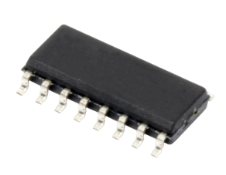
Analog Devices Inc.The MAX6070/MAX6071 offer a very low noise and low-drift voltage reference in a small 6-pin SOT23 package. These devices provide a 1/f noise voltage of only4.8µVP-P at an output voltage of 2.5V, with a temperature drift of 6ppm/°C (max, A grade). The devices consume 150µA of supply current and can sink and source up to 10mA of load current. The low-drift and low-noise specifications enable enhanced system accuracy, making these devices ideal for high-precision industrial applications. The MAX6070 offers a noise filter option for wideband applications.The devices are available in a 6-pin SOT23 package and specified over the extended industrial temperature range of -40°C to +125°C. The 2.5V options are alsoavailable in a 6-bump 0.78mm x 1.41mm wafer-level package (WLP).ApplicationsHigh-Accuracy Industrial and Process ControlHigh-Resolution ADCs and DACsPrecision Current SourcesPrecision Instrumentation
MAX6070BAUT12/V+T
Part Number : MAX6070BAUT12/V+T
Analog Devices Inc.The MAX6070/MAX6071 offer a very low noise and low-drift voltage reference in a small 6-pin SOT23 package. These devices provide a 1/f noise voltage of only4.8µVP-P at an output voltage of 2.5V, with a temperature drift of 6ppm/°C (max, A grade). The devices consume 150µA of supply current and can sink and source up to 10mA of load current. The low-drift and low-noise specifications enable enhanced system accuracy, making these devices ideal for high-precision industrial applications. The MAX6070 offers a noise filter option for wideband applications.The devices are available in a 6-pin SOT23 package and specified over the extended industrial temperature range of -40°C to +125°C. The 2.5V options are alsoavailable in a 6-bump 0.78mm x 1.41mm wafer-level package (WLP).ApplicationsHigh-Accuracy Industrial and Process ControlHigh-Resolution ADCs and DACsPrecision Current SourcesPrecision Instrumentation
MAX6071AAUT25+T
Part Number : MAX6071AAUT25+T
Analog Devices Inc.The MAX6070/MAX6071 offer a very low noise and low-drift voltage reference in a small 6-pin SOT23 package. These devices provide a 1/f noise voltage of only4.8µVP-P at an output voltage of 2.5V, with a temperature drift of 6ppm/°C (max, A grade). The devices consume 150µA of supply current and can sink and source up to 10mA of load current. The low-drift and low-noise specifications enable enhanced system accuracy, making these devices ideal for high-precision industrial applications. The MAX6070 offers a noise filter option for wideband applications.The devices are available in a 6-pin SOT23 package and specified over the extended industrial temperature range of -40°C to +125°C. The 2.5V options are alsoavailable in a 6-bump 0.78mm x 1.41mm wafer-level package (WLP).ApplicationsHigh-Accuracy Industrial and Process ControlHigh-Resolution ADCs and DACsPrecision Current SourcesPrecision Instrumentation
MAX16126EVKIT#
Part Number : MAX16126EVKIT#
Analog Devices Inc.The MAX16126/MAX16127 load-dump/reverse-voltage protection circuits protect power supplies from damaging input voltage conditions, including overvoltage, reverse-voltage, and high-voltage transient pulses. Using a built-in charge pump, the devices control two external back-to-back n-channel MOSFETs that turn off and isolate downstream power supplies during damaging input conditions, such as an automotive load-dump pulse or a reverse-battery condition. Operation is guaranteed down to 3V to ensure proper operation during automotive cold-crank conditions. These devices feature a flag output (active-low FLAG) that asserts during fault conditions.For reverse-voltage protection, external back-to-back MOSFETs outperform the traditional reverse-battery diode, minimizing the voltage drop and power dissipation during normal operation.The MAX16126/MAX16127 use external resistors to adjust the overvoltage and undervoltage comparator thresholds for maximum flexibility.The MAX16127 provides limiter-mode fault management for overvoltage and thermal shutdown conditions; whereas the MAX16126 provides switch-mode fault management for overvoltage and thermal shutdown conditions. In the limiter mode, the output voltage is limited and active-low FLAG is asserted low during a fault. In the switch mode, the external MOSFETs are switched off and active-low FLAG is asserted low after a fault. The switch mode is available in four options: latch mode, 1 autoretry mode, 3 autoretry mode, and always autoretry mode.The MAX16126/MAX16127 are available in 12-pin TQFN packages. These devices operate over the automotive temperature range (-40°C to +125°C).ApplicationsAutomotiveAvionicsIndustrialTelecom/Server/Networking
MAX16930BAGLS/VY+
Part Number : MAX16930BAGLS/VY+
Analog Devices Inc.The MAX16930/MAX16931 offer two high-voltage, synchronous step-down controllers and a step-up preboost controller. They operate with an input voltage supply from 2V to 42V with preboost active and can operate in drop-out condition by running at 95% duty cycle. The devices are intended for applications with mid- to high-power requirements that operate at a wide input voltage range such as during automotive cold-crank or engine stop-start conditions. The MAX16930/MAX16931 step-down controllers operate 180° out-of-phase at frequencies up to 2.2MHz to allow small external components, reduced output ripple, and to guarantee no AM band interference. The switching frequency is resistor adjustable. The FSYNC input programmability enables three frequency modes for optimized performance: forced fixed-frequency operation, skip mode with ultra-low quiescent current (20µA), and synchronization to an external clock. The devices also provide a spread-spectrum option to minimize EMI interference. The MAX16930/MAX16931 are offered with an asynchronous step-up controller. This preboost circuitry turns on during low input voltage conditions. It is designed to provide power to step-down controller channels with input voltages as low as 2V. The devices also feature a power-OK monitor and overvoltage and undervoltage lockout. Protection features include cycle-by-cycle current limit and thermal shutdown. The devices are available in 40-pin TQFN-EP and side-wettable QFND-EP packages and are specified for operation over the -40°C to +125°C automotive temperature range.ApplicationsDistributed DC Power SystemsNavigation and Radio Head UnitsPOL Applications for Automotive Power
MAX16939ATESB/V+T
Part Number : MAX16939ATESB/V+T
Analog Devices Inc.The MAX16935/MAX16939 are 3.5A current-mode step-down converters with integrated high-side and low-side MOSFETs designed to operate with an external Schottky diode for better efficiency. The low-side MOSFET enables fixed-frequency forced-PWM (FPWM) operation under light-load applications. The devices operate with input voltages from 3.5V to 36V, while using only 28µA quiescent current at no load. The switching frequency is resistor programmable from 220kHz to 2.2MHz and can be synchronized to an external clock. The devices’ output voltage is available as 3.3V/5V fixed or adjustable from 1V to 10V. The wide input voltage range along with its ability to operate at 98% duty cycle during undervoltage transients make the devices ideal for automotive and industrial applications.Under light-load applications, the FSYNC logic input allows the devices to either operate in skip mode for reduced current consumption or fixed-frequency FPWM mode to eliminate frequency variation to minimize EMI. Fixed-frequency FPWM mode is extremely useful for power supplies designed for RF transceivers where tight emission control is necessary. Protection features include cycle-by-cycle current limit and thermal shutdown with automatic recovery. Additional features include a power-good monitor to ease power-supply sequencing and a 180° out-of-phase clock output relative to the internal oscillator at SYNCOUT to create cascaded power supplies with multiple devices. The MAX16935/MAX16939 operate over the -40°C to +125°C automotive temperature range and are available in 16-pin (5mm × 5mm) TQFN-EP and 16-pin TSSOP-EP packages.ApplicationsDistributed DC Power SystemsNavigation and Radio Head UnitsPoint-of-Load Applications
MAX16948AGEE/V+T
Part Number : MAX16948AGEE/V+T
Analog Devices Inc.The MAX16948 is a dual high-voltage, current-sensing low dropout linear regulator (LDO)/switch designed to operate with an input voltage range from 4.5V to 28V (45V load dump tolerant). The device provides phantom power over coax cable to remote radio frequency low-noise amplifiers (LNAs) in automotive systems with a maximum current of 300mA per channel. The device also provides a fixed regulated output voltage of 8.5V or an adjustable 1V to 12.5V output voltage. The device can also be configured as a switch.The device monitors the load current and provides an analog output current proportional to the sensed load current. Accurate internal current limits protect the input supply against both overcurrent and short-circuit conditions. The device features an open-drain error output for each channel to indicate to the microcontroller (µC) when a fault has occurred.The device features short-to-battery protection to latch off the internal LDO/switch during a short-to-battery event. During a thermal overload, the device reduces power dissipation by going into thermal shutdown. It includes two independent active-low, high-voltage-compatible shutdown inputs to place each channel in a low-power shutdown mode.The device is available in a 16-pin TQFN package with exposed pad, a 16-pin QSOP package with exposed pad, or a 16-pin QSOP package and is fully specified over the -40°C to +105°C temperature range.ApplicationsAutomotive Camera and Sensor PowerRemote LNA Phantom Power
MAX16956AUBA+T
Part Number : MAX16956AUBA+T
Analog Devices Inc.The MAX16956 is a small, synchronous buck converter with integrated high-side and low-side switches. The device is designed to deliver up to 300mA with input voltages from 3.5V to 36V, while using only 1.1µA quiescent current at no load (fixed-output versions). Voltage quality can be monitored by observing the active-low RESET signal. The device can operate near dropout by running at 97% duty cycle, making it ideal for automotive applications under cold-crank.The device offers fixed-output voltages of 5V and 3.3V, as well as an adjustable version. The adjustable version allows the user to program the output voltage between 1V and 15V by using a resistor-divider. Frequency is fixed at 2.1MHz, which allows for small external components, reduced output ripple, and minimized AM radio interference. The device offers both forced-PWM and skip modes of operation, with ultra-low quiescent current of 1.1µA in skip mode. The device can be ordered with spread-spectrum frequency modulation designed to minimize EMI-radiated emissions due to the switching frequency.The MAX16956 is available in a small (3mm × 3mm) 10-pin µMAX® package and operates across the full automotive temperature range of -40°C to +125°C. The device is AEC-Q100 qualified.ApplicationsAutomotive Body ECUsDistributed DC Power SystemsPoint-of-Load Applications
MAX16956AUBB+
Part Number : MAX16956AUBB+
Analog Devices Inc.The MAX16956 is a small, synchronous buck converter with integrated high-side and low-side switches. The device is designed to deliver up to 300mA with input voltages from 3.5V to 36V, while using only 1.1µA quiescent current at no load (fixed-output versions). Voltage quality can be monitored by observing the active-low RESET signal. The device can operate near dropout by running at 97% duty cycle, making it ideal for automotive applications under cold-crank.The device offers fixed-output voltages of 5V and 3.3V, as well as an adjustable version. The adjustable version allows the user to program the output voltage between 1V and 15V by using a resistor-divider. Frequency is fixed at 2.1MHz, which allows for small external components, reduced output ripple, and minimized AM radio interference. The device offers both forced-PWM and skip modes of operation, with ultra-low quiescent current of 1.1µA in skip mode. The device can be ordered with spread-spectrum frequency modulation designed to minimize EMI-radiated emissions due to the switching frequency.The MAX16956 is available in a small (3mm × 3mm) 10-pin µMAX® package and operates across the full automotive temperature range of -40°C to +125°C. The device is AEC-Q100 qualified.ApplicationsAutomotive Body ECUsDistributed DC Power SystemsPoint-of-Load Applications
MAX16969DGEE/V+T
Part Number : MAX16969DGEE/V+T
Analog Devices Inc.The MAX16969 provides high-ESD and short-circuit protection for the low-voltage internal USB data and USB power line in automotive radio, navigation, connectivity, and USB hub applications. The device supports both Hi-Speed USB (480Mbps) and full-speed USB (12Mbps) operation. In addition, the device also includes integrated circuitry to enable fast-charging for consumer devices adhering to either the Apple method or the Hi-Speed USB host-charger port-detection protocol.The short-circuit protection features include short-to-battery on the protected HVBUS, HVD+, and HVD- outputs, as well as short-to-HVBUS on the protected HVD+ and HVD- outputs. The device is capable of a short-to-battery condition of up to +18V. Short-to-GND and overcurrent protection are also provided on the HVBUS output to protect the internal BUS power rail from overcurrent faults.The device features high-ESD protection to ±15kV Air Gap method and ±8kV Contact method on all protected HVBUS, HVD+, and HVD- outputs.The device features two low 4.0Ω on-resistance Hi-Speed USB switches, a current-limited low-voltage 22mΩ BUS switch, and provides an integrated high-voltage external power-switch controller. The BUS switch can start up into large capacitive noncompliant USB loads. The device also features an enable input, a fault output, integrated Apple iPod®/iPhone® fast-charging termination resistors, and an integrated host-charger port-detection circuit adhering to the USB 2.0 battery charging specification.The device is available in a 16-pin QSOP package, and operates over -40°C to +105°C temperature range.ApplicationsAutomotive USB ProtectionRapid Charging for Apple-Compliant Devices
MAX16984SATI/V+T
Part Number : MAX16984SATI/V+T
Analog Devices Inc.The MAX16984 combines a 5V automotive-grade step-down converter capable of driving up to 2.5A, a USB host charger adapter emulator, and USB protection switches for automotive USB host applications. The USB protection switches provide high-ESD, short-circuit protection and feature integrated host-charger port-detection circuitry adhering to the USB 2.0 Battery Charging Specification BC1.2 battery charging specification and Chinese Telecommunication Industry Standard YD/T 1591-2009. They also include circuitry for iPod®/iPhone® 1.0A and iPad® 2.1A dedicated charging modes. The HVD+ and HVD- ESD protection features include protection to ±15kV Air/±8kV Contact on the HVD+ and HVD- outputs to the IEC 61000-4-2 model and 330Ω, 330pF ESD model. The high-efficiency step-down DC-DC converter operates from a voltage up to 28V and is protected from load dump transients up to 42V. The device is optimized for high-frequency operation and includes resistor-programmable frequency selection from 220kHz to 2.2MHz to allow optimization of efficiency, noise, and board space based on application requirements. The converter has an internal high-side n-channel switch and uses a low forward-drop freewheeling Schottky diode for rectification. There is a small low-side n-channel switch to maintain fixed frequency under light loads. For lower quiescent current operation requirements, the low-side n-channel switch can be disabled to allow skip mode operation under light loads. The converter can deliver up to 2.1A of continuous current at 105°C. The MAX16984S has an integrated spread-spectrum oscillator to improve EMI performance. The MAX16984 also includes a USB load current-sense amplifier and configurable feedback adjustment circuit designed to provide automatic USB voltage adjustment to compensate for voltage drops in captive cables associated with automotive applications. The MAX16984 limits the USB load current using both a fixed internal peak current threshold of the DC-DC converter and a user-configurable external USB load current-sense amplifier threshold.ApplicationsAutomotive ConnectivityAutomotive Radio and NavigationDedicated USB Power ChargerTelematicsUSB Port for Host and Hub Applications
MAX16993AGJL/VY+T
Part Number : MAX16993AGJL/VY+T
Analog Devices Inc.The MAX16993 power-management integrated circuit (PMIC) is a 2.1MHz, multichannel, DC-DC converter designed for automotive applications. The device integrates three supplies in a small footprint. The device includes one high-voltage step-down controller (OUT1) designed to run directly from a car battery and two low-voltage step-down converters (OUT2/OUT3) cascaded from OUT1. Under no-load conditions, the MAX16993 consumes only 30µA of quiescent current, making it ideal for automotive applications.The high-voltage synchronous step-down DC-DC controller (OUT1) operates from a voltage up to 36V continuous and is protected from load-dump transients up to 42V. There is a pin-selectable frequency option of either 2.1MHz or a factory-set frequency for 1.05MHz, 525kHz, 420kHz, or 350kHz. The low-voltage, synchronous step-down DC-DC converters run directly from OUT1 and can supply output currents up to 3A. The device provides a spread-spectrum enable input (SSEN) to provide quick improvement in electromagnetic interference when needed. There is also a SYNC input for providing an input to synchronize to an external clock source (see the Selector Guide in the full data sheet). The device includes overtemperature shutdown and overcurrent limiting. The device also includes individual active-low RESET_ outputs and individual enable inputs. The active-low RESET_ outputs provide voltage monitoring for all output channels.The MAX16993 is available in a 32-pin TQFN/side-wettable QFND-EP package and is specified for operation over the -40°C to +125°C automotive temperature range.ApplicationsAutomotiveIndustrial
MAX17501AATB+T
Part Number : MAX17501AATB+T
Analog Devices Inc.The MAX17501 high-efficiency, high-voltage, synchronous step-down DC-DC converter with integrated MOSFETs operates over a 4.5V to 60V input voltage range. This device is offered in a fixed 3.3V , 5V or adjustable output voltage (0.9V to 92%VIN) while delivering up to 500mA of current. The output voltage is accurate to within ±1.7% over -40°C to +125°C. The MAX17501 is available in a compact TDFN package. Simulation models are available.The device features peak-current-mode control with pulse-width modulation (PWM). Users can choose devices with either pulse frequency modulation (PFM) or forced PWM scheme. PFM devices skip pulses at light load for higher efficiency, while forced-PWM devices operate with fixed switching frequency at any load for noise sensitive-applications. The low-resistance, on-chip MOSFETs ensure high efficiency at full load and simplify the layout.A programmable soft-start feature allows users to reduce input inrush current. The device also incorporates an output enable/undervoltage lockout pin (EN/UVLO) that allows the user to turn on the part at the desired input-voltage level. An open-drain active-low RESET pin provides a delayed power-good signal to the system upon achieving successful regulation of the output voltage.ApplicationsBase Station, VOIP, TelecomBattery-Powered EquipmentGeneral-Purpose Point-of-LoadHome TheaterHVAC and Building ControlIndustrial Process Control
MAX17501EATB+T
Part Number : MAX17501EATB+T
Analog Devices Inc.The MAX17501 high-efficiency, high-voltage, synchronous step-down DC-DC converter with integrated MOSFETs operates over a 4.5V to 60V input voltage range. This device is offered in a fixed 3.3V , 5V or adjustable output voltage (0.9V to 92%VIN) while delivering up to 500mA of current. The output voltage is accurate to within ±1.7% over -40°C to +125°C. The MAX17501 is available in a compact TDFN package. Simulation models are available.The device features peak-current-mode control with pulse-width modulation (PWM). Users can choose devices with either pulse frequency modulation (PFM) or forced PWM scheme. PFM devices skip pulses at light load for higher efficiency, while forced-PWM devices operate with fixed switching frequency at any load for noise sensitive-applications. The low-resistance, on-chip MOSFETs ensure high efficiency at full load and simplify the layout.A programmable soft-start feature allows users to reduce input inrush current. The device also incorporates an output enable/undervoltage lockout pin (EN/UVLO) that allows the user to turn on the part at the desired input-voltage level. An open-drain active-low RESET pin provides a delayed power-good signal to the system upon achieving successful regulation of the output voltage.ApplicationsBase Station, VOIP, TelecomBattery-Powered EquipmentGeneral-Purpose Point-of-LoadHome TheaterHVAC and Building ControlIndustrial Process Control
MAX17501FATB+T
Part Number : MAX17501FATB+T
Analog Devices Inc.The MAX17501 high-efficiency, high-voltage, synchronous step-down DC-DC converter with integrated MOSFETs operates over a 4.5V to 60V input voltage range. This device is offered in a fixed 3.3V , 5V or adjustable output voltage (0.9V to 92%VIN) while delivering up to 500mA of current. The output voltage is accurate to within ±1.7% over -40°C to +125°C. The MAX17501 is available in a compact TDFN package. Simulation models are available.The device features peak-current-mode control with pulse-width modulation (PWM). Users can choose devices with either pulse frequency modulation (PFM) or forced PWM scheme. PFM devices skip pulses at light load for higher efficiency, while forced-PWM devices operate with fixed switching frequency at any load for noise sensitive-applications. The low-resistance, on-chip MOSFETs ensure high efficiency at full load and simplify the layout.A programmable soft-start feature allows users to reduce input inrush current. The device also incorporates an output enable/undervoltage lockout pin (EN/UVLO) that allows the user to turn on the part at the desired input-voltage level. An open-drain active-low RESET pin provides a delayed power-good signal to the system upon achieving successful regulation of the output voltage.ApplicationsBase Station, VOIP, TelecomBattery-Powered EquipmentGeneral-Purpose Point-of-LoadHome TheaterHVAC and Building ControlIndustrial Process Control
MAX17601AUA+
Part Number : MAX17601AUA+
Analog Devices Inc.The MAX17600–MAX17605 devices are high-speed MOSFET drivers capable of sinking /sourcing 4A peak currents. The devices have various inverting and noninverting part options that provide greater flexibility in controlling the MOSFET. The devices have internal logic circuitry that prevents shoot-through during output-state changes. The logic inputs are protected against voltage spikes up to +14V, regardless of VDD voltage. Propagation delay time is minimized and matched between the dual channels. The devices have very fast switching time, combined with short propagation delays (12ns typ), making them ideal for high-frequency circuits. The devices operate from a +4V to +14V single power supply and typically consume 1mA of supply current. The MAX17600/MAX17601 have standard TTL input logic levels, while the MAX17603 /MAX17604/MAX17605 have CMOS-like high-noise margin (HNM) input logic levels. The MAX17600/MAX17603 are dual inverting input drivers, the MAX17601/MAX17604 are dual noninverting input drivers, and the MAX17602/MAX17605 devices have one noninverting and one inverting input. These devices are provided with enable pins (ENA, ENB) for better control of driver operation.These devices are available in 8-pin (3mm x 3mm) TDFN, 8-pin (3mm x 5mm) µMAX®, and 8-pin SO packages and operate over the -40°C to +125°C temperature range.ApplicationsDC-DC ConvertersMotor ControlPower MOSFET SwitchingPower-Supply ModulesSwitch-Mode Power Supplies
REF198FSZ
Part Number : REF198FSZ
Analog Devices Inc.The REF19x series precision band gap voltage references use a patented temperature drift curvature correction circuit and laser trimming of highly stable, thin-film resistors to achieve a very low temperature coefficient and high initial accuracy.The REF19x series is made up of micropower, low dropout voltage (LDV) devices, providing stable output voltage from supplies as low as 100 mV above the output voltage and consuming less than 45 μA of supply current. In sleep mode, which is enabled by applying a low TTL or CMOS level to the SLEEP pin, the output is turned off and supply current is further reduced to less than 15 μA.The REF19x series references are specified over the extended industrial temperature range (−40°C to +85°C) with typical performance specifications over −40°C to +125°C for applications, such as automotive.All electrical grades are available in an 8-lead SOIC package; the PDIP and TSSOP packages are available only in the lowest electrical grade.APPLICATIONS Portable instruments ADCs and DACs Smart sensors Solar powered applications Loop-current-powered instruments
5962-88764043A
Part Number : 5962-88764043A
Analog Devices Inc.The AD7824 and AD7828 are high-speed, multichannel, 8-bit ADCs with a choice of 4 (AD7824) or 8 (AD7828) multiplexed analog inputs. A half-flash conversion technique gives a fast conversion rate of 2.5 µs per channel and the parts have a built-in track/hold function capable of digitizing full-scale signals of 10 kHz (157 mV/µs slew rate) on all channels. The AD7824 and AD7828 operate from a single +5 V supply and have an analog input range of 0 V to +5 V, using an external +5 V reference.Microprocessor interfacing of the parts is simple, using standard Chip Select (CS) and Read (RD) signals to initiate the conversion and read the data from the three-state data outputs. The half-flash conversion technique means that there is no need to generate a clock signal for the ADC. The AD7824 and AD7828 can be interfaced easily to most popular microprocessors.The AD7824 and AD7828 are fabricated in an advanced, all ion-implanted, Linear-Compatible CMOS process (LC2MOS) and have low power dissipation of 40 mW (typ). The AD7824 is available in a 0.3' wide, 24-pin 'skinny' DIP, while the AD7828 is available in a 0.6' wide, 28-pin DIP and in 28- terminal surface mount packages.
AD5204BRUZ100-R7
Part Number : AD5204BRUZ100-R7
Analog Devices Inc.The AD5204/AD5206 provide 4-/6-channel, 256-position digitally controlled variable resistor (VR) devices. These devices perform the same electronic adjustment function as a potentiometer or variable resistor. Each channel of the AD5204/AD5206 contains a fixed resistor with a wiper contact that taps the fixed resistor value at a point determined by a digital code loaded into the SPI-compatible serial-input register. The resistance between the wiper and either endpoint of the fixed resistor varies linearly with respect to the digital code transferred into the VR latch. The variable resistor offers a completely programmable value of resistance between the A terminal and the wiper or the B terminal and the wiper. The fixed A-to-B terminal resistance of 10 kΩ, 50 kΩ, or 100 kΩ has a nominal temperature coefficient of 700 ppm/°C.Each VR has its own VR latch that holds its programmed resistance value. These VR latches are updated from an internal serial-to-parallel shift register that is loaded from a standard 3-wire serial-input digital interface. Eleven data bits make up the data-word clocked into the serial input register. The first three bits are decoded to determine which VR latch is loaded with the last eight bits of the data-word when the CS strobe is returned to logic high. A serial data output pin at the opposite end of the serial register (AD5204 only) allows simple daisy chaining in multiple VR applications without requiring additional external decoding logic.An optional reset (PR) pin forces all the AD5204 wipers to the midscale position by loading 0x80 into the VR latch.The AD5204/AD5206 are available in the 24-lead surface-mount SOIC and TSSOP packages. The AD5204 is also available in a 32-lead, 5 mm × 5 mm LFCSP package. All parts are guaranteed to operate over the extended industrial temperature range of −40°C to +85°C. For additional single-, dual-, and quad-channel devices, see the AD8400/AD8402/AD8403 data sheets.APPLICATIONS Mechanical potentiometer replacement Instrumentation: gain, offset adjustment Programmable voltage-to-current conversion Programmable filters, delays, time constants Line impedance matching
MAX5522EUA+
Part Number : MAX5522EUA+
Analog Devices Inc.The MAX5522-MAX5525 are dual, 10-bit, ultra-lowpower,voltage-output, digital-to-analog converters(DACs) offering rail-to-rail buffered voltage outputs. TheDACs operate from a 1.8V to 5.5V supply and consumeless than 5µA, making the devices suitable for lowpowerand low-voltage applications. A shutdown modereduces overall current, including the reference inputcurrent, to just 0.18µA. The MAX5522-MAX5525 use a3-wire serial interface that is compatible with SPI,QSPI, and MICROWIRE.Upon power-up, the MAX5522-MAX5525 outputs aredriven to zero scale, providing additional safety forapplications that drive valves or for other transducersthat need to be off during power-up. The zero-scaleoutputs enable glitch-free power-up.The MAX5522 accepts an external reference input andprovides unity-gain outputs. The MAX5523 contains aprecision internal reference and provides a bufferedexternal reference output with unity-gain DAC outputs.The MAX5524 accepts an external reference input andprovides force-sense outputs. The MAX5525 contains aprecision internal reference and provides a bufferedexternal reference output with force-sense DAC outputs.The MAX5524/MAX5525 are available in a 4mm x 4mmx 0.8mm, 12-pin, thin QFN package. The MAX5522/MAX5523 are available in an 8-pin µMAX package. Alldevices are guaranteed over the extended -40°C to+85°C temperature range.For 12-bit compatible devices, refer to the MAX5532-MAX5535 data sheet. For 8-bit compatible devices,refer to the MAX5512-MAX5515 data sheet.ApplicationsAutomatic Trimming and Calibration in Factory or FieldChemical Sensor Cell Bias for Gas MonitorsIndustrial Process Control and Remote Industrial DevicesPortable Battery-Powered Devices InstrumentationProgrammable LCD BiasProgrammable Voltage and Current SourcesRemote Data Conversion and Monitoring


