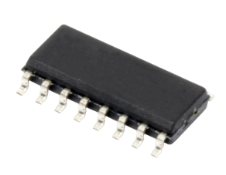
LTC3831EGN#PBF
Part Number : LTC3831EGN#PBF
Analog Devices Inc.The LTC3831 is a high power, high efficiency switching regulator controller designed for DDR memory termination. The LTC3831 generates an output voltage equal to 1/2 of an external supply or reference voltage. The LTC3831 uses a synchronous switching architecture with N-channel MOSFETs. Additionally, the chip senses output current through the drain-source resistance of the upper N-channel FET, providing an adjustable current limit without a current sense resistor.The LTC3831 operates with input supply voltage as low as 3V and with a maximum duty cycle of >91%. It includes a fixed frequency PWM oscillator for low output ripple operation. The 200kHz free-running clock frequency can be externally adjusted or synchronized with an external signal from 100kHz to above 500kHz. In shutdown mode, the LTC3831 supply current drops to
MAX1133BEAP+
Part Number : MAX1133BEAP+
Analog Devices Inc.The MAX1132/MAX1133 are 200ksps, 16-bit ADCs. These serially interfaced ADCs connect directly to SPI™, QSPI™, and MICROWIRE™ devices without external logic. They combine an input scaling network, internal track/hold, clock, a +4.096V reference, and three general-purpose digital output pins (for external multiplexer or PGA control) in a 20-pin SSOP package. The excellent dynamic performance (SINAD > 85dB), high-speed (200ksps), and low power (7.5mA) of these ADCs, make them ideal for applications such as industrial process control, instrumentation, and medical applications. The MAX1132 accepts input signals of 0 to +12V (unipolar) or ±12V (bipolar), while the MAX1133 accepts input signals of 0 to +4.096V (unipolar) or ±4.096V (bipolar). Operating from a single +4.75V to +5.25V analog supply and a +4.75V to +5.25V digital supply, power-down modes reduce current consumption to 1mA at 10ksps and further reduce supply current to less than 20µA at slower data rates. A serial strobe output (SSTRB) allows direct connection to the TMS320 family of digital signal processors. The MAX1132/MAX1133 user can select either the internal clock, or an external serial-interface clock for the ADC to perform analog-to-digital conversions.The MAX1132/MAX1133 feature internal calibration circuitry to correct linearity and offset errors. On-demand calibration allows the user to optimize performance. Three user-programmable logic outputs are provided for the control of an 8-channel mux or a PGA.ApplicationsData AcquisitionIndustrial I/O ModulesIndustrial Process ControlsMedical InstrumentsPortable Battery-Powered Equipment
MAX1480EACPI+
Part Number : MAX1480EACPI+
Analog Devices Inc.The MAX1480EA/MAX1480EC/MAX1490EA/MAX1490EB are complete, electrically isolated, RS-485/RS-422 data communications interface solutions in a hybrid microcircuit. The RS-485/RS-422 I/O pins are protected against ±15kV electrostatic discharge (ESD) shocks, without latchup. Transceivers, optocouplers, and a transformer provide a complete interface in a standard DIP package. A single +5V supply on the logic side powers both sides of the interface.The MAX1480EC/MAX1490EB feature reduced-slew-rate drivers that minimize EMI and reduce reflections caused by improperly terminated cables, allowing error-free data transmission at data rates up to 160kbps. The MAX1480EA/MAX1490EA driver slew rate is not limited, allowing transmission rates up to 2.5Mbps. The MAX1480EA/MAX1480EC are designed for half-duplex communication, while the MAX1490EA/MAX1490EB feature full-duplex communication.Drivers are short-circuit current limited and protected against excessive power dissipation by thermal shutdown circuitry that places the driver outputs into a high-impedance state. The receiver input has a fail-safe feature that guarantees a known output (RO low for the MAX1480EA/MAX1480EC, active-low RO high for the MAX1490EA/ MAX1490EB) if the input is open circuit.The MAX1480EA/MAX1480EC/MAX1490EA/MAX1490EB withstand 1260VRMS (1min) or 1520VRMS (1s). Their isolated outputs meet all RS-485/RS-422 specifications. The MAX1480EA/MAX1480EC are available in a 28-pin DIP package, and the MAX1490EA/MAX1490EB are available in a 24-pin DIP package.ApplicationsAutomated Test Equipment (ATE)HVAC/Building Control NetworksIndustrial Control Local Area NetworksIsolated RS-485/RS-422 Data InterfaceTelecomTransceivers for EMI-Sensitive Applications
MAX1480EAEPI+
Part Number : MAX1480EAEPI+
Analog Devices Inc.The MAX1480EA/MAX1480EC/MAX1490EA/MAX1490EB are complete, electrically isolated, RS-485/RS-422 data communications interface solutions in a hybrid microcircuit. The RS-485/RS-422 I/O pins are protected against ±15kV electrostatic discharge (ESD) shocks, without latchup. Transceivers, optocouplers, and a transformer provide a complete interface in a standard DIP package. A single +5V supply on the logic side powers both sides of the interface.The MAX1480EC/MAX1490EB feature reduced-slew-rate drivers that minimize EMI and reduce reflections caused by improperly terminated cables, allowing error-free data transmission at data rates up to 160kbps. The MAX1480EA/MAX1490EA driver slew rate is not limited, allowing transmission rates up to 2.5Mbps. The MAX1480EA/MAX1480EC are designed for half-duplex communication, while the MAX1490EA/MAX1490EB feature full-duplex communication.Drivers are short-circuit current limited and protected against excessive power dissipation by thermal shutdown circuitry that places the driver outputs into a high-impedance state. The receiver input has a fail-safe feature that guarantees a known output (RO low for the MAX1480EA/MAX1480EC, active-low RO high for the MAX1490EA/ MAX1490EB) if the input is open circuit.The MAX1480EA/MAX1480EC/MAX1490EA/MAX1490EB withstand 1260VRMS (1min) or 1520VRMS (1s). Their isolated outputs meet all RS-485/RS-422 specifications. The MAX1480EA/MAX1480EC are available in a 28-pin DIP package, and the MAX1490EA/MAX1490EB are available in a 24-pin DIP package.ApplicationsAutomated Test Equipment (ATE)HVAC/Building Control NetworksIndustrial Control Local Area NetworksIsolated RS-485/RS-422 Data InterfaceTelecomTransceivers for EMI-Sensitive Applications
MAX8510EXK28+T
Part Number : MAX8510EXK28+T
Analog Devices Inc.The MAX8510/MAX8511/MAX8512 ultra-low-noise, low-dropout (LDO) linear regulators are designed to deliver up to 120mA continuous output current. These regulators achieve a low 120mV dropout for 120mA load current. The MAX8510 uses an advanced architecture to achieve ultra-low output voltage noise of 11µVRMS and PSRR of 54dB at 100kHz.The MAX8511 does not require a bypass capacitor, hence achieving the smallest PC board area. The MAX8512's output voltage can be adjusted with an external divider.The MAX8510/MAX8511 are preset to a variety of voltages in the 1.5V to 4.5V range. Designed with a P-channel MOSFET series pass transistor, the MAX8510/MAX8511/MAX8512 maintain very low ground current (40µA).The regulators are designed and optimized to work with low-value, low-cost ceramic capacitors. The MAX8510 requires only 1µF (typ) of output capacitance for stability with any load. When disabled, current consumption drops to below 1µA.Package options include a 5-pin SC70 and a tiny 2mm x 2mm x 0.8mm TDFN package.ApplicationsBase StationsBluetooth® Portable Radios and AccessoriesCellular and Cordless PhonesDigital CamerasPDA and Palmtop ComputersPersonal StereosPortable and Battery-Powered EquipmentWireless LANs
MAX8517EUB+
Part Number : MAX8517EUB+
Analog Devices Inc.The MAX8516/MAX8517/MAX8518 low-dropout linear regulators operate from input voltages as low as 1.425V and are able to deliver up to 1A of continuous outputcurrent with a maximum dropout voltage of only 200mV. The output voltage can be set from 0.5V to (VIN - 0.2V) and is 1.4% accurate over load and line variations, from 0°C to +85°C.These regulators use small, 1µF ceramic input capacitors and 4.7µF ceramic output capacitors to deliver 1A output current. High bandwidth provides excellent transient response and limits the output voltage deviation to 45mV for a 20mA to 1A load step, with only a 4.7µF ceramic output capacitor, and the voltage deviations can be reduced further by increasing the output capacitor.Designed with an internal p-channel MOSFET pass transistor, the MAX8516/MAX8517/MAX8518 feature low 340µA (typ) supply current during dropout conditions.Soft-start reduces inrush current. Other features include a logic-controlled shutdown mode, short-circuit protection, and thermal-overload protection.The MAX8517 features a power-OK (POK) output that transitions high when the regulator output is within ±10% of its nominal output voltage. The MAX8518 features a 150ms power-on reset output.The parts are packaged in a 10-pin µMAX® package that includes an exposed pad for optimal power dissipation.ApplicationsAutomated Test Equipment (ATE)NetworkingNotebooksOptical ModulesPDAsPost RegulatorsServersStorageWireless Base Stations
MAX9176EUB+T
Part Number : MAX9176EUB+T
Analog Devices Inc.The MAX9176/MAX9177 are 670MHz, low-jitter, low-skew, 2:1 multiplexers ideal for protection switching, loopback, and clock distribution. The devices feature ultra-low 68ps peak-to-peak deterministic jitter that ensures reliable operation in high-speed links that are highly sensitive to timing errors.The MAX9176 has fail-safe LVDS inputs and an LVDS output. The MAX9177 has 'anything' differential inputs (CML/LVDS/LVPECL) and an LVDS output. The output can be put into high impedance using the power-down input. The MAX9176 features fail-safe circuits that drive the output high when a selected input is open, undriven and shorted, or undriven and terminated. The MAX9177 has bias circuits that force the output high when a selected input is open. The mux select and power-down inputs are compatible with standard LVTTL/LVCMOS logic.The select and power-down inputs tolerate -1V undershoot and VCC + 1V overshoot. The MAX9176/MAX9177 are available in 10-pin µMAX and 10-pin thin QFN packages, and operate from a single 3.3V supply over the -40°C to +85°C temperature range.ApplicationsClock DistributionLoopbackProtection Switching
MAX9700AEUB+T
Part Number : MAX9700AEUB+T
Analog Devices Inc.The MAX9700 mono class D audio power amplifier provides class AB amplifier performance with class D efficiency, conserving board space and extending battery life. Using a class D architecture, the MAX9700 delivers 1.2W into an 8Ω load while offering efficiencies above 90%. A low-EMI modulation scheme renders the traditional class D output filter unnecessary.The MAX9700 offers two modulation schemes: a fixed-frequency (FFM) mode, and a spread-spectrum mode that reduces EMI-radiated emissions due to the modulation frequency. Furthermore, the MAX9700 oscillator can be synchronized to an external clock through the SYNC input, allowing the switching frequency to beuser defined. The SYNC input also allows multiple MAX9700s to be cascaded and frequency locked, minimizing interference due to clock intermodulation. The device utilizes a fully differential architecture, a full-bridged output, and full-bridged comprehensive click-and-pop suppression. The gain of the MAX9700 is set internally (MAX9700A: 6dB, MAX9700B: 12dB, MAX9700C: 15.6dB, MAX9700D: 20dB), further reducing external component count.The MAX9700 features high 72dB PSRR, a low 0.01% THD+N, and SNR in excess of 90dB. Short-circuit and thermal-overload protection prevent the device from damage during a fault condition. The MAX9700 is available in 10-pin TDFN (3mm x 3mm x 0.8mm), 10-pin µMAX® and 12-bump UCSP™ (1.5mm x 2mm x 0.6mm) packages. The MAX9700 is specified over the extended -40°C to +85°C temperature range.ApplicationsCell PhonesMP3 PlayersPDAsPortable Audio
MAX9716EUA+
Part Number : MAX9716EUA+
Analog Devices Inc.The MAX9716/MAX9717 audio power amplifiers are ideal for portable audio devices with internal speakers. A bridge-tied load (BTL) architecture minimizes externalcomponent count, while providing high-quality audio reproduction. Both devices deliver 1.4W continuous power into a 4Ω load with less than 1% Total Harmonic Distortion (THD) while operating from a single +5V supply. With an 8Ω load, both devices deliver 1W continuous power. These devices also deliver 350mW continuous power into an 8Ω load while operating from a single +3.0V supply. The devices are available as adjustable gain amplifiers (MAX9716/MAX9717A) or with internally fixed gains of 6dB, 9dB, and 12dB (MAX9717B/MAX9717C/MAX9717D), reducing component count.A low-power shutdown mode disables the bias generator and amplifiers, reducing quiescent current consumption to less than 10nA. These devices feature Maxim'sindustry-leading, comprehensive click-and-pop suppression that reduces audible clicks and pops during startup and shutdown.The MAX9717 features a headphone sense input (active-low BTL/SE) that senses when a headphone is connected to the device, disables the BTL slave driver, muting the speaker while driving the headphone as a single-ended load. The MAX9716 is pin compatible with the LM4890 and is available in 9-bump UCSP™, 8-pin TDFN (3mm x 3mm), and 8-pin µMAX® packages. The MAX9717 is available in 9-bump UCSP, 8-pin TDFN, and 8-pin µMAX packages. Both devices operate over the -40°C to +85°C extended temperature range.ApplicationsMobile PhonesPDAsPortable Devices
MAX9717AETA+T
Part Number : MAX9717AETA+T
Analog Devices Inc.The MAX9716/MAX9717 audio power amplifiers are ideal for portable audio devices with internal speakers. A bridge-tied load (BTL) architecture minimizes externalcomponent count, while providing high-quality audio reproduction. Both devices deliver 1.4W continuous power into a 4Ω load with less than 1% Total Harmonic Distortion (THD) while operating from a single +5V supply. With an 8Ω load, both devices deliver 1W continuous power. These devices also deliver 350mW continuous power into an 8Ω load while operating from a single +3.0V supply. The devices are available as adjustable gain amplifiers (MAX9716/MAX9717A) or with internally fixed gains of 6dB, 9dB, and 12dB (MAX9717B/MAX9717C/MAX9717D), reducing component count.A low-power shutdown mode disables the bias generator and amplifiers, reducing quiescent current consumption to less than 10nA. These devices feature Maxim'sindustry-leading, comprehensive click-and-pop suppression that reduces audible clicks and pops during startup and shutdown.The MAX9717 features a headphone sense input (active-low BTL/SE) that senses when a headphone is connected to the device, disables the BTL slave driver, muting the speaker while driving the headphone as a single-ended load. The MAX9716 is pin compatible with the LM4890 and is available in 9-bump UCSP™, 8-pin TDFN (3mm x 3mm), and 8-pin µMAX® packages. The MAX9717 is available in 9-bump UCSP, 8-pin TDFN, and 8-pin µMAX packages. Both devices operate over the -40°C to +85°C extended temperature range.ApplicationsMobile PhonesPDAsPortable Devices
MAX9722AETE+T
Part Number : MAX9722AETE+T
Analog Devices Inc.The MAX9722A/MAX9722B stereo headphone amplifiers are designed for portable equipment where board space is at a premium. The MAX9722A/MAX9722B use aunique DirectDrive® architecture to produce a ground-referenced output from a single supply, eliminating the need for large DC-blocking capacitors, which saves cost, board space, and component height. Additionally, the gain of the amplifier is set internally (-2V/V, MAX9722B) or adjusted externally (MAX9722A). The MAX9722A/MAX9722B deliver up to 70mW per channel into a 16Ω load or 130mW into a 32Ω load and have low 0.009% THD+N. An 80dB at 217Hz power-supply rejection ratio (PSRR) allows these devices to operate from noisy digital supplies without an additional linear regulator. The MAX9722A/MAX9722B include ±8kV ESD protection on the headphone outputs. Comprehensive anticlick-and-pop circuitry suppresses audible clicks and pops on startup and shutdown. A low-power shutdown mode reduces the supply current to 0.1µA.The MAX9722A/MAX9722B operate from a single 2.4V to 5.5V supply, consume only 5.5mA of supply current, feature short-circuit and thermal-overload protection,and are specified over the extended -40°C to +85°C temperature range. The devices are available in tiny 16-pin thin QFN (3mm x 3mm x 0.8mm) and 16-pinTSSOP packages.ApplicationsCell PhonesFlat-Panel MonitorsMP3 PlayersNotebook and Desktop PCsPDAsPortable Audio EquipmentSmartphones
MAX1873REEE+
Part Number : MAX1873REEE+
Analog Devices Inc.The low-cost MAX1873R/S/T provides all functions needed to simply and efficiently charge 2-, 3-, or 4-series lithium-ion cells at up to 4A or more. It provides a regulated charging current and voltage with less than ±0.75% total voltage error at the battery terminals. An external P-channel MOSFET operates in a step-down DC-DC configuration to efficiently charge batteries in low-cost designs.The MAX1873R/S/T regulates the battery voltage and charging current using two control loops that work together to transition smoothly between voltage and current regulation. An additional control loop limits current drawn from the input source so that AC adapter size and cost can be minimized. An analog voltage output proportional to charging current is also supplied so that an ADC or microcontroller can monitor charging current.The MAX1873 may also be used as an efficient current-limited source to charge NiCd or NiMH batteries in multichemistry charger designs. The MAX1873R/S/T is available in a space-saving 16-pin QSOP package. Use the evaluation kit (MAX1873EVKIT) to help reduce design time.Applications2-, 3-, or 4-Cell Li+ Battery Pack Chargers6-, 9-, or 10-Cell Li+ Battery Pack ChargersDesktop Cradle ChargersHandheld Instruments (PDAs, Palmtops)Notebook ComputersPortable Desktop Assistants (PDAs)Portable Internet Tablets
MAX1953EUB+
Part Number : MAX1953EUB+
Analog Devices Inc.The MAX1953/MAX1954/MAX1957 is a family of versatile, economical, synchronous current-mode, pulse-width modulation (PWM) buck controllers. These step-down controllers are targeted for applications where cost and size are critical.The MAX1953 operates at a fixed 1MHz switching frequency, thus significantly reducing external component size and cost. Additionally, excellent transient response is obtained using less output capacitance. The MAX1953 operates from low 3V to 5.5V input voltage and can supply up to 10A of output current. Selectable current limit is provided to tailor to the external MOSFETs' on-resistance for optimum cost and performance. The output voltage is adjustable from 0.8V to 0.86VIN.With the MAX1954, the drain-voltage range on the high- side FET is 3V to 13.2V and is independent of the supply voltage. It operates at a fixed 300kHz switching frequency and can be used to provide up to 25A of output current with high efficiency. The output voltage is adjustable from 0.8V to 0.86VHSD.The MAX1957 features a tracking output voltage range of 0.4V to 0.86VIN and is capable of sourcing or sinking current for applications such as DDR bus termination and PowerPC®/ASIC/DSP core supplies. The MAX1957 operates from a 3V to 5.5V input voltage and at a fixed 300kHz switching frequency. The MAX1953/MAX1954/MAX1957 provide a COMP pin that can be pulled low to shut down the converter in addition to providing compensation to the error amplifier. An input undervoltage lockout (UVLO) is provided to ensure proper operation under power-sag conditions to prevent the external power MOSFETs from overheating. Internal digital soft-start is included to reduce inrush current. The MAX1953/MAX1954/MAX1957 are available in tiny 10-pin µMAX packages.ApplicationsGraphic Cards and Video CardsLow-Voltage Distributed PowerMicroprocessor Core SuppliesPCs and ServersPrinters and ScannersTelecommunications and Networking
MAX1969EUI+
Part Number : MAX1969EUI+
Analog Devices Inc.The MAX1968/MAX1969 are highly integrated and cost-effective, high-efficiency, switch-mode drivers for Peltier thermoelectric cooler (TEC) modules. Both devices utilize direct current control to eliminate current surges in the TEC. On-chip FETs minimize external components while providing high efficiency. A 500kHz/1MHz switching frequency and a unique ripple cancellation scheme reduce component size and noise.The MAX1968 operates from a single supply and provides bipolar ±3A output by biasing the TEC between the outputs of two synchronous buck regulators. Bipolar operation allows for temperature control without 'dead zones' or other nonlinearities at low load currents. This arrangement ensures that the control system does not hunt when the set point is very close to the natural operating point, requiring a small amount of heating or cooling. An analog control signal precisely sets the TEC current. The MAX1969 provides unipolar output up to 6A. Reliability is optimized with settable limits for bothTEC voltage and current, with independently set limits for heating and cooling current. An analog output also monitors TEC current.The MAX1968/MAX1969 are available in a low-profile 28-pin TSSOP-EP package and is specified over the -40°C to +85°C temperature range. The thermally-enhanced TSSOP-EP package with exposed metal pad minimizes operating junction temperature. An evaluation kit is available to speed designs.ApplicationsAutomated Test Equipment (ATE)Biotech Lab EquipmentEDFA Optical AmplifiersFiber Optic Network EquipmentFiber-Optic Laser ModulesTelecom Fiber InterfacesWDM, DWDM Laser Diode Temperature Control
MAX1972EEE+
Part Number : MAX1972EEE+
Analog Devices Inc.The MAX1970/MAX1971/MAX1972 dual-output current-mode PWM buck regulators operate from 2.6V to 5.5V input and deliver a minimum of 750mA on each output. The MAX1970 and MAX1972 operate at a fixed 1.4MHz (MAX1971 operates at 700kHz) to reduce output inductor and capacitor size and cost. Switching the regulators 180° out-of-phase also reduces the input capacitor size and cost. Ceramic capacitors can be used for input and output. The output voltages are programmable from 1.2V to VIN using external feedback resistors, or can be preset to 1.8V or 3.3V for output 1 and 1.5V or 2.5V for output 2. When one output is higher than 1.2V, the second can be configured down to sub-1V levels. Output accuracy is better than ±1% over variations in load, line, and temperature. Internal soft-start reduces inrush current during startup.All devices feature power-on reset (active-low POR). The MAX1971 includes a reset input (RSI), which forces active-low POR low for 175ms after RSI goes low. The MAX1970 and MAX1972 include an open-drain power-fail output (PFO) that monitors input voltage and goes high when the input falls below 3.94V. For USB-powered xDSL modems, this output can be used to detect USB power failure. A minimum switching frequency of 1.2MHz ensures operation outside the xDSL band.Learn More AboutPowerMind™ApplicationsCopper Gigabit SFP and GBIC ModulesDual LDO ReplacementUSB-Powered DevicesXDSL ModemsxDSL Routers
MAX1982EUT+T
Part Number : MAX1982EUT+T
Analog Devices Inc.The MAX1982/MAX1983 are low-voltage, low-dropout linear regulators with an external bias supply input. The 5V bias supply drives the gate of the internal N-channel pass transistor, making these devices ideal for applications that require low-voltage outputs from low-voltage inputs. The MAX1982 delivers 1.2V (±3%) at 300mA from an input voltage of 1.25V to 5.5V. The MAX1983 delivers an adjustable output voltage from 0.8V to 2V.The MAX1982/MAX1983 include a current-limit and thermal shutdown that protects the regulator in the event of a fault condition. Both devices are offered in a 6-pin SOT23 package and are specified over the extended (-40°C to +85°C) temperature range.ApplicationsCell PhonesLow-Dropout Regulators with External Bias SupplyNotebook ComputersPDAsVID Power Supplies
MAX202CSE+
Part Number : MAX202CSE+
Analog Devices Inc.MAX200-MAX209, MAX211, and MAX213 are a family of RS-232 and V.28 transceivers with integrated charge pump circuitry for single +5V supply operation.The drivers maintain the ±5V EIA/TIA-232E output signal levels at data rates in excess of 120kbps when loaded in accordance with the EIA/TIA-232E specification.The MAX211 and MAX213 are available in a 28-pin, wide small-outline (SO) package and a 28-pin shrink small- outline (SSOP) package, which occupies only 40% of the area of the SO. The MAX207 is available in a 24-pin SO package and a 24-pin SSOP. The MAX203 and MAX205 use no external components and are recommended for applications with limited circuit board space.ApplicationsBattery-Powered EquipmentHandheld EquipmentPortable Diagnostics Equipment
MAX3040CSE+
Part Number : MAX3040CSE+
Analog Devices Inc.The MAX3040–MAX3045 is a family of 5V quad RS-485/RS-422 transmitters designed for digital data transmission over twisted-pair balanced lines. All transmitter outputs are protected to ±10kV using the Human Body Model. The MAX3040/MAX3043 (250kbps) and the MAX3041/MAX3044 (2.5Mbps) are slew-rate limited transmitters that minimize EMI and reduce reflections caused by improperly terminated cables, thus allowing error-free transmission.The MAX3040–MAX3045 feature a hot-swap capability that eliminates false transitions on the data cable during power-up or hot insertion. The MAX3042B/MAX3045B are optimized for data transfer rates up to 20Mbps, the MAX3041/MAX3044 for data rates up to 2.5Mbps, and the MAX3040/MAX3043 for data rates up to 250kbps. The MAX3040–MAX3045 offer optimum performance when used with the MAX3093E or MAX3095 5V quad differential line receivers or MAX3094E/MAX3096 3V quad differential line receivers. The MAX3040–MAX3045 are ESD-protected pin-compatible, low-power upgrades to the industry-standard 'SN75174 and 'DS26LS31C. They are available in space-saving TSSOP, narrow SO, and wide SO packages.ApplicationsHandheld EquipmentIndustrial Motor ControlIndustrial PLCsNetworkingTelecommunications EquipmentTransmitter for ESD-Sensitive Applications
MAX3041EUE+
Part Number : MAX3041EUE+
Analog Devices Inc.The MAX3040–MAX3045 is a family of 5V quad RS-485/RS-422 transmitters designed for digital data transmission over twisted-pair balanced lines. All transmitter outputs are protected to ±10kV using the Human Body Model. The MAX3040/MAX3043 (250kbps) and the MAX3041/MAX3044 (2.5Mbps) are slew-rate limited transmitters that minimize EMI and reduce reflections caused by improperly terminated cables, thus allowing error-free transmission.The MAX3040–MAX3045 feature a hot-swap capability that eliminates false transitions on the data cable during power-up or hot insertion. The MAX3042B/MAX3045B are optimized for data transfer rates up to 20Mbps, the MAX3041/MAX3044 for data rates up to 2.5Mbps, and the MAX3040/MAX3043 for data rates up to 250kbps. The MAX3040–MAX3045 offer optimum performance when used with the MAX3093E or MAX3095 5V quad differential line receivers or MAX3094E/MAX3096 3V quad differential line receivers. The MAX3040–MAX3045 are ESD-protected pin-compatible, low-power upgrades to the industry-standard 'SN75174 and 'DS26LS31C. They are available in space-saving TSSOP, narrow SO, and wide SO packages.ApplicationsHandheld EquipmentIndustrial Motor ControlIndustrial PLCsNetworkingTelecommunications EquipmentTransmitter for ESD-Sensitive Applications
MAX3044ESE+T
Part Number : MAX3044ESE+T
Analog Devices Inc.The MAX3040–MAX3045 is a family of 5V quad RS-485/RS-422 transmitters designed for digital data transmission over twisted-pair balanced lines. All transmitter outputs are protected to ±10kV using the Human Body Model. The MAX3040/MAX3043 (250kbps) and the MAX3041/MAX3044 (2.5Mbps) are slew-rate limited transmitters that minimize EMI and reduce reflections caused by improperly terminated cables, thus allowing error-free transmission.The MAX3040–MAX3045 feature a hot-swap capability that eliminates false transitions on the data cable during power-up or hot insertion. The MAX3042B/MAX3045B are optimized for data transfer rates up to 20Mbps, the MAX3041/MAX3044 for data rates up to 2.5Mbps, and the MAX3040/MAX3043 for data rates up to 250kbps. The MAX3040–MAX3045 offer optimum performance when used with the MAX3093E or MAX3095 5V quad differential line receivers or MAX3094E/MAX3096 3V quad differential line receivers. The MAX3040–MAX3045 are ESD-protected pin-compatible, low-power upgrades to the industry-standard 'SN75174 and 'DS26LS31C. They are available in space-saving TSSOP, narrow SO, and wide SO packages.ApplicationsHandheld EquipmentIndustrial Motor ControlIndustrial PLCsNetworkingTelecommunications EquipmentTransmitter for ESD-Sensitive Applications


