
ADP2120ACPZ-1.5-R7
Part Number : ADP2120ACPZ-1.5-R7
Analog Devices Inc.The ADP2119 / ADP2120 are low quiescent current, synchronous, step-down DC-to -DC regulators in a compact 3mm x3mm LFCSP_WD package. Both Devices use current mode, constant frequency pulse-width modulation (PWM) control scheme for excellent stability and transient response. Under light load condition, they can be configured to operate in pulse frequency modulation (PFM) mode that reduces switching frequency to save power.The ADP2119/ADP2120 can support input voltages from 2.3V to 5.5V. The output voltage can be adjusted from 0.6V to input voltage (VIN) for the adjustable version, while the fixed output version is available in preset output voltage options of 3.3V, 2.5V, 1.8V, 1.5V ,1.2V and 1.0V. The ADP2119/ADP2120 require minimal external parts and provide a high efficiency solution with their integrated power switches, synchronous rectifier, and internal compensation. Each IC draws less than 3 μA current from the input source when it is disabled. Other key features include under voltage lockout(UVLO), integrated soft start to limit inrush current at startup, overvoltage protection (OVP), over current protection (OCP) and thermal shutdown (TSD).APPLICATIONS Point of load conversion Communications and networking equipment Industrial and instrumentation Consumer electronics Medical appliances
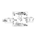
DC2105A-B
Part Number : DC2105A-B
Analog Devices Inc.Power Management IC Development Tools LTC3630AEMSE/LTC3630EMSE Demo Board - Hi
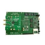
DC1564A-A
Part Number : DC1564A-A
Analog Devices Inc.Data Conversion IC Development Tools LTC2157-14: 14-bit, 250Msps, 1.8V Dual A

SSM2135SZ
Part Number : SSM2135SZ
Analog Devices Inc.The SSM2135 dual audio operational amplifier permits excel-lent performance in portable or low power audio systems, with an operating supply range of 4 V to 36 V or ±2 V to ±18 V. The unity-gain stable device has very low voltage noise of 5.2 nV/√Hz, and total harmonic distortion plus noise below 0.01% over normal signal levels and loads. Such characteristics are enhanced by wide output swing and load drive capability. A unique output stage1 permits output swing approaching the rail under moderate load conditions. Under severe loading, the SSM2135 still maintains a wide output swing with ultralow distortion. Particularly well suited for computer audio systems and portable digital audio units, the SSM2135 can perform preamplification, headphone and speaker driving, and balanced line driving and receiving. Additionally, the device is ideal for input signal conditioning in single-supply, Σ-Δ, analog-to-digital converter subsystems such as the AD1877. The SSM2135 makes an ideal single-supply stereo output amplifier for audio digital-to-analog converters (DACs) because of its low noise and distortion.The SSM2135 is available in an 8-lead plastic SOIC package and is guaranteed for operation over the extended industrial temperature range of −40°C to +85°C.
LTM8032MPY
Part Number : LTM8032MPY
Analog Devices Inc.Switching Voltage Regulators EN55022B Compliant 36V, 2A DC/DC Modul

SSM6322ACPZ-R2
Part Number : SSM6322ACPZ-R2
Analog Devices Inc.The SSM6322 is an integrated, dual-channel audio amplifier solution that interfaces directly with audio DAC/CODEC, maximizing the fidelity of high fidelity audio signal chains. The highly efficient design of the SSM6322 delivers outstandingaudio performance while minimizing power dissipation for maximum battery life in portable applications.The SSM6322 features −121 dB THD + N at 1 kHz, along with very low output noise from 20 Hz to 20 kHz. The low power operation, high peak output current, and high PSRR make the SSM6322 an ideal candidate for applications that require high fidelity audio, high dynamic range, precision, and low power. This highly integrated drive solution also reduces development time while reducing board space and minimizing external components.The SSM6322 is available in a 24-lead LFCSP package. The SSM6322 operates over the industrial temperature of −40°C to +85°C.Applications High fidelity headphone driver Mobile phones Bluetooth speakers & headphones Gaming Notebooks and Tablets A/V receivers Professional audio equipment Audio test equipment Automobile infotainment system

AD5689BRUZ
Part Number : AD5689BRUZ
Analog Devices Inc.The AD5689/AD5687 members of the nanoDAC+™ family arelow power, dual, 16-/12-bit, buffered voltage output digital-to-analogconverters (DACs). The devices include a gain select pingiving a full-scale output of 2.5 V (gain = 1) or 5 V (gain = 2). TheAD5689/AD5687 operate from a single 2.7 V to 5.5 V supply, areguaranteed monotonic by design, and exhibit less than 0.1% FSRgain error and 1.5 mV offset error performance. Both devices areavailable in a 3 mm × 3 mm LFCSP and a TSSOP package.The AD5689/AD5687 also incorporate a power-on reset circuitand a RSTSEL pin that ensures that the DAC outputs power upto zero scale or midscale and remain there until a valid writetakes place. Each part contains a per channel power-down featurethat reduces the current consumption of the device to 4 µA at3 V while in power-down mode.The AD5689/AD5687 uses a versatile serial peripheral interfacethat operates at clock rates up to 50 MHz. Both devices containa VLOGIC pin that is intended for 1.8 V/3 V/5 V logic.Product Highlights High Relative Accuracy (INL). AD5689 (16-bit): ±2 LSB maximum Excellent DC Performance. Total unadjusted error: ±0.1% of FSR maximum Offset error: ±1.5 mV maximum Gain error: ±0.1% of FSR maximum Two Package Options. 3 mm × 3 mm, 16-lead LFCSP or 16-lead TSSOPApplications Optical transceivers Base station power amplifiers Process control (PLC I/O cards) Industrial automation Data acquisition systems

AD5700-1BCPZ-R5
Part Number : AD5700-1BCPZ-R5
Analog Devices Inc.The AD5700/AD5700-1 are single-chip solutions, designedand specified to operate as a HART® FSK half-duplex modem,complying with the HART physical layer requirements. TheAD5700/AD5700-1 integrate all of the necessary filtering, signaldetection, modulating, demodulating and signal generationfunctions, thus requiring few external components. The 0.5%precision internal oscillator on the AD5700-1 greatly reducesthe board space requirements, making it ideal for line-poweredapplications in both master and slave configurations. The maximumsupply current consumption is 115µA, making theAD5700/AD5700-1 an optimal choice for low power loop-powered applications.Transmit waveforms are phase continuous 1200 Hz and2200 Hz sinusoids. The AD5700/AD5700-1 contain accuratecarrier detect circuitry and use a standard UART interface.Applications Field transmitters HART multiplexers PLC and DCS analog I/O modules HART network connectivity

AD5700BCPZ-R5
Part Number : AD5700BCPZ-R5
Analog Devices Inc.The AD5700/AD5700-1 are single-chip solutions, designedand specified to operate as a HART® FSK half-duplex modem,complying with the HART physical layer requirements. TheAD5700/AD5700-1 integrate all of the necessary filtering, signaldetection, modulating, demodulating and signal generationfunctions, thus requiring few external components. The 0.5%precision internal oscillator on the AD5700-1 greatly reducesthe board space requirements, making it ideal for line-poweredapplications in both master and slave configurations. The maximumsupply current consumption is 115µA, making theAD5700/AD5700-1 an optimal choice for low power loop-powered applications.Transmit waveforms are phase continuous 1200 Hz and2200 Hz sinusoids. The AD5700/AD5700-1 contain accuratecarrier detect circuitry and use a standard UART interface.Applications Field transmitters HART multiplexers PLC and DCS analog I/O modules HART network connectivity
AD5700BCPZ-RL7
Part Number : AD5700BCPZ-RL7
Analog Devices Inc.The AD5700/AD5700-1 are single-chip solutions, designedand specified to operate as a HART® FSK half-duplex modem,complying with the HART physical layer requirements. TheAD5700/AD5700-1 integrate all of the necessary filtering, signaldetection, modulating, demodulating and signal generationfunctions, thus requiring few external components. The 0.5%precision internal oscillator on the AD5700-1 greatly reducesthe board space requirements, making it ideal for line-poweredapplications in both master and slave configurations. The maximumsupply current consumption is 115µA, making theAD5700/AD5700-1 an optimal choice for low power loop-powered applications.Transmit waveforms are phase continuous 1200 Hz and2200 Hz sinusoids. The AD5700/AD5700-1 contain accuratecarrier detect circuitry and use a standard UART interface.Applications Field transmitters HART multiplexers PLC and DCS analog I/O modules HART network connectivity

AD7609BSTZ
Part Number : AD7609BSTZ
Analog Devices Inc.The AD7609 is an 18-bit, 8-channel, true differential, simultaneous sampling analog-to-digital data acquisition system (DAS). The part contains analog input clamp protection, a second-order antialiasing filter, a track-and-hold amplifier, an 18-bit charge redistribution successive approximation analog-to-digital converter (ADC), a flexible digital filter, a 2.5 V reference and reference buffer, and high speed serial and parallel interfaces.The AD7609 operates from a single 5 V supply and can accommodate ±20 V and ±10 V true bipolar differential input signals while sampling at throughput rates up to 200 kSPS for all channels. The input clamp protection circuitry can tolerate voltages up to ±16.5 V on each analog input pin. The AD7609 has 1 MΩ analog input impedance regardless of sampling frequency. The single supply operation, on-chip filtering, and high input impedance eliminate the need for driver op amps and external bipolar supplies. The AD7609 antialiasing filter has a −3 dB cutoff frequency of 32 kHz and provides 40 dB antialias rejection when sampling at 200 kSPS. The flexible digital filter is pin driven, yields improvements in SNR, and reduces the −3 dB bandwidth. Applications Power line monitoring and protection systems Multiphase motor control Instrumentation and control systems Multiaxis positioning systems Data acquisition systems (DAS)

AD7988-5BCPZ-RL
Part Number : AD7988-5BCPZ-RL
Analog Devices Inc.The AD7988-1/AD7988-5 are 16-bit, successive approximation,analog-to-digital converters (ADC) that operate from a singlepower supply, VDD. The AD7988-1 offers a 100 kSPS throughput,and the AD7988-5 offers a 500 kSPS throughput. They are lowpower, 16-bit sampling ADCs with a versatile serial interfaceport. On the CNV rising edge, they sample an analog input,IN+, between 0 V to VREF with respect to a ground sense, IN−.The reference voltage, REF, is applied externally and can be setindependent of the supply voltage, VDD.The SPI-compatible serial interface also features the ability todaisy-chain several ADCs on a single 3-wire bus using the SDIinput. It is compatible with 1.8 V, 2.5 V, 3 V, or 5 V logic usingthe separate supply, VIO.The AD7988-1/AD7988-5 generics are housed in a 10-leadMSOP or a 10-lead LFCSP with operation specified from −40°Cto +125°C.Applications Automated test equipment Data acquisition systems Medical instruments Machine automation

AD8229HRZ
Part Number : AD8229HRZ
Analog Devices Inc.The AD8229 is an ultralow noise instrumentation amplifierdesigned for measuring small signals in the presence of largecommon-mode voltages and high temperatures.The AD8229 has been designed for high temperature operation. The process is dielectrically isolated to avoid leakage currents at high temperatures. The design architecture was chosen to compensate for the low VBE voltages at high temperatures.The AD8229 excels at measuring tiny signals. It delivers industry leading 1 nV/√Hz input noise performance. The high CMRR of the AD8229 prevents unwanted signals from corrupting theacquisition. The CMRR increases as the gain increases, offering high rejection when it is most needed. The AD8229 is one of the fastest instrumentation amplifiersavailable. Its current feedback architecture provides high bandwidth at high gain, for example, 1.2 MHz at G = 100. Thedesign includes circuitry to improve settling time after largeinput voltage transients. The AD8229 was designed for excellentdistortion performance, allowing use in demanding applicationssuch as vibration analysis.Gain is set from 1 to 1000 with a single resistor. A reference pinallows the user to offset the output voltage. This feature can be useful when interfacing with analog-to-digital converters.For the most demanding applications, the AD8229 is availablein an 8-lead side-brazed ceramic dual in-line package (SBDIP).For space-constrained applications, the AD8229 is available inan 8-lead plastic standard small outline package (SOIC).The AD8229 is also available as Known Good DieApplications Down-hole instrumentation Harsh environment data acquisition Exhaust gas measurements Vibration analysis

AD8421ARMZ-RL
Part Number : AD8421ARMZ-RL
Analog Devices Inc.The AD8421 is a low cost, low power, extremely low noise, ultralow bias current, high speed instrumentation amplifier that is ideally suited for a broad spectrum of signal conditioning and data acquisition applications. This product features extremely high CMRR, allowing it to extract low level signals in the presence of high frequency common-mode noise over a wide temperature range. The 10 MHz bandwidth, 35 V/µs slew rate, and 0.6 µs settling time to 0.001% (G = 10) allow the AD8421 to amplify high speed signals and excel in applications that require high channel count, multiplexed systems. Even at higher gains, the current feedback architecture maintains high performance; for example, at G = 100, the bandwidth is 2 MHz and the settling time is 0.8 µs. The AD8421 has excellent distortion performance, making it suitable for use in demanding applications such as vibration analysis. The AD8421 delivers industry-leading 3 nV/√Hz input voltage noise and 200 fA/√Hz current noise with only 2 mA quiescent current, making it an ideal choice for measuring low level signals. For applications with high source impedance, the AD8421 employs innovative process technology and design techniques to provide noise performance that is limited only by the sensor. The AD8421 uses unique protection methods to ensure robust inputs while still maintaining very low noise. This protection allows input voltages up to 40 V from the opposite supply rail without damage to the part. A single resistor sets gains between 1 and 10,000. The reference pin can be used to apply a precise offset to the output voltage.The AD8421 performance is specified from −40°C to +85°C for the 8-lead MSOP and SOIC packages, and from −40°C to 125°C for the 8-lead LFCSP package.Applications Medical instrumentation Precision data acquisition Microphone preamplification Vibration analysis Multiplexed input applications ADC driver
AD8421TRMZ-EP-R7
Part Number : AD8421TRMZ-EP-R7
Analog Devices Inc.The AD8421 is a low cost, low power, extremely low noise, ultralow bias current, high speed instrumentation amplifier that is ideally suited for a broad spectrum of signal conditioning and data acquisition applications. This product features extremely high CMRR, allowing it to extract low level signals in the presence of high frequency common-mode noise over a wide temperature range. The 10 MHz bandwidth, 35 V/µs slew rate, and 0.6 µs settling time to 0.001% (G = 10) allow the AD8421 to amplify high speed signals and excel in applications that require high channel count, multiplexed systems. Even at higher gains, the current feedback architecture maintains high performance; for example, at G = 100, the bandwidth is 2 MHz and the settling time is 0.8 µs. The AD8421 has excellent distortion performance, making it suitable for use in demanding applications such as vibration analysis. The AD8421 delivers industry-leading 3 nV/√Hz input voltage noise and 200 fA/√Hz current noise with only 2 mA quiescent current, making it an ideal choice for measuring low level signals. For applications with high source impedance, the AD8421 employs innovative process technology and design techniques to provide noise performance that is limited only by the sensor. The AD8421 uses unique protection methods to ensure robust inputs while still maintaining very low noise. This protection allows input voltages up to 40 V from the opposite supply rail without damage to the part. A single resistor sets gains between 1 and 10,000. The reference pin can be used to apply a precise offset to the output voltage.The AD8421 performance is specified from −40°C to +85°C for the 8-lead MSOP and SOIC packages, and from −40°C to 125°C for the 8-lead LFCSP package.Applications Medical instrumentation Precision data acquisition Microphone preamplification Vibration analysis Multiplexed input applications ADC driver

AD8422ARMZ-RL
Part Number : AD8422ARMZ-RL
Analog Devices Inc.The AD8422 is a high precision, low power, low noise, rail-to-rail instrumentation amplifier that delivers the best performance per unit microampere in the industry. The AD8422 processes signals with ultralow distortion performance that is load independent over its full output range.The AD8422 is the third generation development of the industry standard AD620. The AD8422 employs new process technologies and design techniques to achieve higher dynamic range and lower errors than its predecessors, while consuming less than one-third of the power. The AD8422 uses the high performance pinout introduced by the AD8221.Very low bias current makes the AD8422 error-free with high source impedance, allowing multiple sensors to be multiplexed to the inputs. Low voltage noise and low current noise make the AD8422 an ideal choice for measuring a Wheatstone bridge.The wide input range and rail-to-rail output of the AD8422 bring all of the benefits of a high performance in-amp to single-supply applications. Whether using high or low supply voltages, the power savings make the AD8422 an excellent choice for high channel count or power sensitive applications.The AD8422 uses robust input protection that ensures reliability without sacrificing noise performance. The AD8422 has high ESD immunity, and the inputs are protected from continuous voltages up to 40 V from the opposite supply rail.A single resistor sets the gain from 1 to 1000. The reference pin can be used to apply a precise offset to the output voltage.The AD8422 is specified from −40°C to +85°C for the 8-lead MSOP and the 8-lead SOIC_N and from −40°C to +125°C for the 8-lead LFCSP.APPLICATIONS Medical instrumentation Industrial process controls Strain gages Transducer interfaces Precision data acquisition systems Channel-isolated systems Portable instrumentation

AD8426BCPZ-R7
Part Number : AD8426BCPZ-R7
Analog Devices Inc.The AD8426 is a dual-channel, low cost, wide supply range instrumentation amplifier that requires only one external resistor to set any gain from 1 to 1000.The AD8426 is designed to work with a variety of signal voltages. A wide input range and rail-to-rail output allow the signal to make full use of the supply rails. Because the input range can also go below the negative supply, small signals near ground can be amplified without requiring dual supplies. The AD8426 operates on supplies ranging from ±1.35 V to ±18 V for dual supplies and 2.2 V to 36 V for a single supply.The robust AD8426 inputs are designed to connect to real-world sensors. In addition to its wide operating range, the AD8426 can handle voltages beyond the rails. For example, with a ±5 V supply, the part is guaranteed to withstand ±35 V at the input with no damage. Minimum and maximum input bias currents are specified to facilitate open-wire detection.The AD8426 is designed to make PCB routing easy and efficient. The two amplifiers are arranged in a logical way so that typical application circuits have short routes and few vias. Unlike most chip scale packages, the AD8426 does not have an exposed metal pad on the bottom of the part, which frees additional space for routing and vias. The AD8426 offers two in-amps in the equivalent board space of a typical MSOP package.The AD8426 is ideal for multichannel, space-constrained industrial applications. Unlike other low cost, low power instrumentation amplifiers, the AD8426 is designed with a minimum gain of 1 and can easily handle ±10 V signals. With its space-saving LFCSP package and 125°C temperature rating, the AD8426 thrives in tightly packed, zero airflow designs.The AD8226 is the single channel version of the AD8426.APPLICATIONSIndustrial process controlsBridge amplifiersMedical instrumentationPortable data acquisitionMultichannel systems

AD8429BRZ
Part Number : AD8429BRZ
Analog Devices Inc.The AD8429 is an ultralow noise, instrumentation amplifier designed for measuring extremely small signals over a wide temperature range (−40°C to +125°C).The AD8429 excels at measuring tiny signals. It delivers ultralow input noise performance of 1 nV/√Hz. The high CMRR of the AD8429 prevents unwanted signals from corrupting the acqui-sition. The CMRR increases as the gain increases, offering high rejection when it is most needed. The high performance pin configuration of the AD8429 allows it to reliably maintain high CMRR at frequencies well beyond those of typical instrumentation amplifiers.The AD8429 reliably amplifies fast changing signals. Its current feedback architecture provides high bandwidth at high gain, for example, 1.2 MHz at G = 100. The design includes circuitry to im-prove settling time after large input voltage transients. The AD8429 was designed for excellent distortion performance, allowing use in demanding applications such as vibration analysis.Gain is set from 1 to 10,000 with a single resistor. A reference pin allows the user to offset the output voltage. This feature can be useful to shift the output level when interfacing to a single supply signal chain.The AD8429 performance is specified over the extended industrial temperature range of −40°C to +125°C. It is available in an 8-lead plastic SOIC package.APPLICATIONSMedical instrumentationPrecision data acquisitionMicrophone preamplificationVibration analysis

AD8450ASTZ
Part Number : AD8450ASTZ
Analog Devices Inc.The AD8450 is a precision analog front end for testing andmonitoring battery cells. Referring to figure one, a precisionprogrammable gain instrumentation amplifier (PGIA)measures the battery’s charge/discharge current and aprogrammable gain difference amplifier (PGDA) measures thebattery’s voltage. Internal laser trimmed resistor networks setthe gains for the PGIA and the PGDA, optimizing the AD8450’sperformance over the rated temperature range. PGIA gains are26×, 66×, 133×, and 200×. PGDA gains are 0.2×, 0.27×,0.4×,and 0.8×.Voltages at the ISET and VSET inputs set the desired constantvoltage (CV) and constant current (CC) values. CC to CVswitching is automatic and transparent to the system.A TTL level logic input, MODE, selects between charge anddischarge modes (high for charge, low for discharge). An analogoutput, VCTRL, interfaces directly with ADI’s ADP1972 &ADP1974 PWM controllers.The AD8450 includes resistor programmable overvoltage andovercurrent detection and current sharing circuitry. Currentsharing is used to balance charge among multiple batteries.The AD8450 simplifies designs by providing excellent accuracy,performance over temperature, flexibility with functionality,and overall reliability in a space-saving package. The AD8450 isavailable in an 80 lead 14 mm ×14 mm × 1 mm LQFP packageand is rated at −40 °C to +85 °C operating temperature.APPLICATIONS Battery cell testing & formation Battery module testing
AD8450ASTZ-RL
Part Number : AD8450ASTZ-RL
Analog Devices Inc.The AD8450 is a precision analog front end for testing andmonitoring battery cells. Referring to figure one, a precisionprogrammable gain instrumentation amplifier (PGIA)measures the battery’s charge/discharge current and aprogrammable gain difference amplifier (PGDA) measures thebattery’s voltage. Internal laser trimmed resistor networks setthe gains for the PGIA and the PGDA, optimizing the AD8450’sperformance over the rated temperature range. PGIA gains are26×, 66×, 133×, and 200×. PGDA gains are 0.2×, 0.27×,0.4×,and 0.8×.Voltages at the ISET and VSET inputs set the desired constantvoltage (CV) and constant current (CC) values. CC to CVswitching is automatic and transparent to the system.A TTL level logic input, MODE, selects between charge anddischarge modes (high for charge, low for discharge). An analogoutput, VCTRL, interfaces directly with ADI’s ADP1972 &ADP1974 PWM controllers.The AD8450 includes resistor programmable overvoltage andovercurrent detection and current sharing circuitry. Currentsharing is used to balance charge among multiple batteries.The AD8450 simplifies designs by providing excellent accuracy,performance over temperature, flexibility with functionality,and overall reliability in a space-saving package. The AD8450 isavailable in an 80 lead 14 mm ×14 mm × 1 mm LQFP packageand is rated at −40 °C to +85 °C operating temperature.APPLICATIONS Battery cell testing & formation Battery module testing


