AD7302BRZ
Part Number : AD7302BRZ
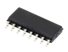
Analog Devices Inc.The AD7302 is a dual, 8-bit voltage out DAC that operates from a single +2.7 V to +5.5 V supply. Its on-chip precision output buffers allow the DAC outputs to swing rail to rail. The AD7302 has a parallel microprocessor and DSP-compatible interface with high speed registers and double buffered interface logic. Data is loaded to the registers on the rising edge of CS or WR and the A/B pin selects either DAC A or DAC B.Reference selection for AD7302 can be either an internal reference derived from the VDD or an external reference applied at the REFIN pin. Both DACs can be simultaneously updated using the asynchronous LDAC input and can be cleared by using the asynchronous CLR input.The low power consumption of this part makes it ideally suited to portable battery operated equipment. The power consumption is less than 10 mW at 3.3 V, reducing to 3 µW in powerdown mode.The AD7302 is available in a 20-pin plastic dual-in-line package, 20-lead SOIC and a 20-lead TSSOP package.APPLICATIONS Portable Battery Powered Instruments Digital Gain and Offset Adjustment Programmable Voltage and Current Sources Programmable AttenuatorsPRODUCT HIGHLIGHTS Low Power, Single Supply Operation. This part operates from a single +2.7 V to +5.5 V supply and typically consumes 15 mW at 5 V, making it ideal for battery powered applications. The on-chip output buffer amplifiers allow the outputs of the DACs to swing rail to rail with a settling time of typically 1.2 µs. Internal or external reference capability. High speed parallel interface. Power-Down Capability. When powered down the DAC consumes less than 1 µA at 25°C. Packaged in 20-lead DIP, SOIC and TSSOP packages.
AD7303BNZ
Part Number : AD7303BNZ
Analog Devices Inc.The AD7303 is a dual, 8-bit voltage out DAC that operates from a single +2.7 V to +5.5 V supply. Its on-chip precision output buffers allow the DAC outputs to swing rail to rail. This device uses a versatile 3-wire serial interface that operates at clock rates up to 30 MHz, and is compatible with QSPI, SPI, microwire and digital signal processor interface standards. The serial input register is sixteen bits wide; 8 bits act as data bits for the DACs, and the remaining eight bits make up a control register.The on-chip control register is used to address the relevant DAC, to power down the complete device or an individual DAC, to select internal or external reference and to provide a synchronous loading facility for simultaneous update of the DAC outputs with a software LDAC function.The low power consumption of this part makes it ideally suited to portable battery operated equipment. The power consumption is 7.5 mW max at 3 V, reducing to less than 3 µW in full power-down mode.The AD7303 is available in an 8-pin plastic dual in-line package, 8-lead SOIC and microSOIC packages.
AD7472ARZ
Part Number : AD7472ARZ
Analog Devices Inc.The AD7470/AD7472 are 10-bit /12-bit high speed, low power, successive-approximation ADCs. The parts operate from a single 2.7 V to 5.25 V power supply and feature throughput rates up to 1.5 MSPS for the 12-bit AD7472 and up to 1.75 MSPS for the 10-bit AD7470. The parts contain a low-noise, wide bandwidth track/hold amplifier which can handleinput frequencies in excess of 20 MHz.The conversion process and data acquisition are controlledusing standard control inputs, allowing easy interfacing tomicroprocessors or DSPs. The input signal is sampled on thefalling edge of CONVST, and conversion is also initiated atthis point. BUSY goes high at the start of conversion andgoes low 531.66 ns after falling edge of CONVST (AD7472with a clock frequency of 26 MHz) to indicate that the conversionis complete. There are no pipeline delays associatedwith the parts. The conversion result is accessed via standardCS and RD signals over a high speed parallel interface.The AD7470/AD7472 use advanced design techniques toachieve very low power dissipation at high throughput rates. With3 V supplies and 1.5 MSPS throughput rates, the AD7470typically consumes, on average, just 1.1 mA. With 5 V suppliesand 1.75 MSPS, the average current consumption is typically1.6 mA. The part also offers flexible power/throughput ratemanagement. Operating the AD7470 with 3 V supplies and500 kSPS throughput reduces the current consumption to 713 μA.At 5 V supplies and 500 kSPS, the part consumes 944 μA.It is also possible to operate the parts in an auto sleep mode,where the part wakes up to do a conversion and automaticallyenters sleep mode at the end of conversion. This method allowsvery low power dissipation numbers at lower throughput rates.In this mode, the AD7472 can be operated with 3 V supplies at100 kSPS, and consume an average current of just 124 μA. At5 V supplies and 100 kSPS, the average current consumption is171 μA.The analog input range for the part is 0 V to REF IN. The 2.5 Vreference is applied externally to the REF IN pin. The conversionrate is determined by the externally-applied clock.ol { margin-top:0px; margin-right:0px; margin-bottom:0px; margin-left:25px; padding-top:0px; padding-right:0px; padding-bottom:10px; padding-left:0px;}li { padding-top:0px; padding-right:0px; padding-bottom:5px; padding-left:0px; margin-top:0px; margin-right:0px; margin-bottom:0px; margin-left:0px;}Product HighlightsHigh Throughput with Low Power Consumption. TheAD7470 offers 1.75 MSPS throughput and the AD7472offers 1.5 MSPS throughput rates with 4 mW powerconsumption.Flexible Power/Throughput Rate Management. The conversionrate is determined by an externally-applied clock allowingthe power to be reduced as the conversion rate is reduced.The part also features an auto sleep mode to maximize powerefficiency at lower throughput rates.No Pipeline Delay. The part features a standard successiveapproximation ADC with accurate control of the samplinginstant via a CONVST input and once off conversion control.
AD767AD
Part Number : AD767AD
Analog Devices Inc.The AD767 is a complete voltage output 12-bit digital-to-analog converter including high stability buried Zener reference and input latch on a single chip. The converter uses 12 precision high-speed bipolar current steering switches and a laser-trimmed thin-film resistor network to provide high accuracy.Microprocessor compatibility is achieved by the on-chip latch. The design of the input latch allows direct interface to 12-bit buses. The latch responds to strobe pulses as short as 40 ns, allowing use with the fastest available microprocessors.The functional completeness and high performance of the AD767 result from a combination of advanced switch design, high-speed bipolar manufacturing process, and the proven laser wafer-trimming (LWT) technology.The subsurface (buried) Zener diode on the chip provides a low-noise voltage reference which has long-term stability and temperature drift characteristics comparable to the best discrete reference diodes. The laser trimming process which provides the excellent linearity is also used to trim the absolute value of the reference as well as its temperature coefficient. The AD767 is thus well suited for wide temperature range performance with ±½ LSB maximum linearity error and guaranteed monotonicity over the full temperature range. Typical full-scale gain is 5 ppm/ºC.
AD795JRZ
Part Number : AD795JRZ
Analog Devices Inc.The AD795 is a low noise, precision, FET input operational amplifier. It offers both the low voltage noise and low offset drift of a bipolar input op amp and the very low bias current of a FET-input device. The 1014 Ω common-mode impedance insures that input bias current is essentially independent of common-mode voltage and supply voltage variations.The AD795 has both excellent dc performance and a guaranteed and tested maximum input voltage noise. It features 2 pA maximum input bias current and 500 μV maximum offset voltage, along with low supply current of 1.5 mA maximum.Furthermore, the AD795 features a guaranteed low input noise of 3.3 μV P-P (0.1 Hz to 10 Hz) and a 11 nV/√Hz maximum noise level at 10 kHz. The AD795 has a fully specified and tested input offset voltage drift of only 10 μV/°C maximum.The AD795 is useful for many high input impedance, low noise applications. The AD795 is rated over the commercial temperature range of 0°C to +70°C.The AD795 is available in an 8-lead SOIC package.Applications Low noise photodiode preamps CT scanners Precision l-to-V converters
AD824ARZ-14-3V-RL
Part Number : AD824ARZ-14-3V-RL
Analog Devices Inc.The AD824 is a quad, FET input, single supply amplifier, featuring rail-to-rail outputs. The combination of FET inputs and rail-to-rail outputs makes the AD824 useful in a wide variety of low voltage applications where low input current is a primary consideration.The AD824 is guaranteed to operate from a 3 V single supply up to ±15 volt dual supplies. AD824AR-3V parametric performance at 3 V is fully guaranteed.Fabricated on ADI's complementary bipolar process, the AD824 has a unique input stage that allows the input voltage to safely extend beyond the negative supply and to the positive supply without any phase inversion or latch-up. The output voltage swings to within 15 mV of the supplies. Capacitive loads to 350 pF can be handled without oscillation.The FET input combined with laser trimming provides an input that has extremely low bias currents with guaranteed offsets below 1 mV. This enables high accuracy designs even with high source impedances. Precision is combined with low noise,making the AD824 ideal for use in battery powered medical equipment.Applications for the AD824 include portable medical equipment, photo diode preamplifiers, and high impedance transducer amplifiers.The ability of the output to swing rail-to-rail enables designers to build multistage filters in single supply systems and maintain high signal-to-noise ratios.The AD824 is specified over the extended industrial (−40°C to +85°C) temperature range and is available in narrow 14-lead SOIC package.Applications Photo diode preamplifier Battery powered instrumentation Power supply control and protection Medical instrumentation Remote sensors Low voltage strain gage amplifiers DAC output amplifier
AD848JRZ
Part Number : AD848JRZ
Analog Devices Inc.The AD848 and AD849 are high speed, low power monolithic operational amplifiers. The AD848 is internally compensated so that it is stable for closed loop gains of 5 or greater. The AD849 is fully decompensated and is stable at gains greater than 24. The AD848 and AD849 achieve their combination of fast ac and good dc performance by utilizing Analog Devices' junction isolated complementary bipolar (CB) process. This process enables these op amps to achieve their high speed while only requiring 4.8 mA of current from the power supplies.The AD848 and AD849 are members of Analog Devices' family of high speed op amps. This family includes, among others, the AD847 which is unity gain stable, with a gain bandwidth of 50 MHz. For more demanding applications, the AD840, AD841 and AD842 offer even greater precision and greater output current drive.The AD848 and AD849 have good dc performance. When operating with ±5 V supplies, they offer open loop gains of 13 V/mV (AD848 with a 500 Ohm load) and low input offset voltage of 1 mV maximum. Common-mode rejection is a minimum of 92 dB. Output voltage swing is ±3 V even into loads as low as 150 Ohm.
AD8522ANZ
Part Number : AD8522ANZ
Analog Devices Inc.The AD8522 is a complete dual 12-bit, single-supply, voltage output DAC in a 14-pin DIP, or SO-14 surface mount package. Fabricated in a CBCMOS process, features include a serial digital interface, onboard reference, and buffered voltage output. Ideal for +5 V-only systems, this monolithic device offers low cost and ease of use, and requires no external components to realize the full performance of the device.The serial digital interface allows interfacing directly to numerous microcontroller ports, with a simple high speed, three-wire data, clock, and load strobe format. The 16-bit serial word contains the 12-bit data word and DAC select address, which is decoded internally or can be decoded externally using LDA, LDB inputs. A serial data output allows the user to easily daisy-chain multiple devices in conjunction with a chip select input. A reset RS input sets the outputs to zero scale or midscale, as determined by the input MSB.The output 4.095 V full scale is laser trimmed to maintain accuracy over the operating temperature range of the device, and gives the user an easy-to-use one-millivolt-per-bit resolution. A 2.5 V reference output is also available externally for other data acquisition circuitry, and for ratiometric applications. The output buffers are capable of driving ±5 mA.The AD8522 is available in the 14-pin plastic DIP and low profile 1.5 mm SOIC-14 packages.APPLICATIONS Digitally Controlled Calibration Servo Controls Process Control Equipment Computer Peripherals Portable Instrumentation Cellular Base Stations Voltage Adjustment
AD8620BRZ-REEL7
Part Number : AD8620BRZ-REEL7
Analog Devices Inc.The AD8610 (single) and AD8620 (dual) are very high precision JFET input amplifiers featuring ultralow offset voltage and drift, very low input voltage and current noise, very low input bias current, and wide bandwidth. Unlike many JFET amplifiers, the AD8610 input bias current is low over the entire operating temperature range. The AD8610 is stable with capacitive loads of over 1000 pF in noninverting unity gain; much larger capacitive loads can be driven easily at higher noise gains. The AD8610 swings to within 1.2 V of the supplies even with a 1 k Ω load, maximizing dynamic range even with limited supply voltages. Outputs slew at 50 V/µs in either inverting or noninverting gain configurations, and settle to 0.01% accuracy in less than 600 ns. Combined with the high input impedance, great precision, and very high output drive, theAD8610 is an ideal amplifier for driving high performance A/D inputs and buffering D/A converter outputs. Applications for the AD8610 and AD8620 include electronic instruments; ATE amplification, buffering, and integrator circuits; CAT/MRI/Ultrasound medical instrumentation; instrumentation quality photodiode amplification; fast precision filters (including PLL filters); and high quality audio. The AD8610 is fully specified over the extended industrial (-40ºC to +125ºC temperature range. The AD8610 is available in the narrow 8-lead SOIC and the tiny MSOP8 surface-mount packages. The AD8620 is available in the narrow 8-lead SOIC package. MSOP8 packaged devices are available only in tape and reel.
DAC8800FPZ
Part Number : DAC8800FPZ
Analog Devices Inc.The DAC-8800 Trim DAC™ is designed to be a general purpose digitally controlled voltage adjustment device. The output voltage range can be independently set for each set of four D/A converters. In addition, both unipolar and bipolar output voltage ranges are easy to establish by external reference input high and low terminals. The digitally-programed output voltages are ideal for op amp trimming, voltage-controlled amplifier gain setting and any general purpose trimming tasks.A three-wire serial digital interface loads the contents of eight internal DAC registers which establish the output voltage levels. An asynchronous Clear (CLR) input places all DACs in a zero code output condition, very handy for system power-up. An internal regulator provides TTl input compatibility over a wide range of VDD supply voltages. Single supply operation is available by connecting VSS to GND.
DC661A-A
Part Number : DC661A-A
Analog Devices Inc.The LT3468/LT3468-1/LT3468-2 are highly integrated ICs designed to charge photoflash capacitors in digital and film cameras. A patented control technique* allows for the use of extremely small transformers. Each device contains an on-chip high voltage NPN power switch. Output voltage detection* is completely contained within the device, eliminating the need for any discrete zener diodes or resistors. The output voltage can be adjusted by simply changing the turns ratio of the transformer. The LT3468 has a primary current limit of 1.4A, the LT3468-2 has a 1A limit, and the LT3468-1 has a 0.7A limit. These different current limit levels result in well controlled input currents of 500mA for the LT3468, 375mA for the LT3468-2 and 225mA for the LT3468-1. Aside from the differing current limit, the three devices are otherwise equivalent.The CHARGE pin gives full control of the part to the user. Driving CHARGE low puts the part in shutdown. The DONE pin indicates when the part has completed charging. The LT3468 series of parts are available in tiny low profile (1mm) SOT-23 packages.Applications Digital / Film Camera Flash PDA / Cell Phone Flash Emergency Strobe
DC757A-A
Part Number : DC757A-A
Analog Devices Inc.The LTC4302-1/LTC4302-2 addressable I2C bus and SMBus compatible bus buffers allow a peripheral board to be inserted and removed from a live backplane without corruption of the bus. The LTC4302-1/LTC4302-2 maintain electrical isolation between the backplane and peripheral board until their VCC supply is valid and a master device on the backplane side addresses the LTC4302-1/LTC4302-2 and commands them to connect. The LTC4302-1/LTC4302-2’s ADDRESS pin provides 32 possible addresses set by an external resistive divider between VCC and GND. The LTC4302-1/LTC4302-2 work with supply voltages ranging from 2.7V to 5.5V. The SDA and SCL inputs and outputs do not load the bus lines when VCC is low.Rise time accelerator circuitry allows for heavier capacitive bus loading while still meeting system timing requirements. During insertion, the SDA and SCL lines are precharged to 1V to minimize bus disturbances. Two general purpose input/output pins (GPIOs) on the LTC4302-1 can be configured as inputs, open-drain outputs or push-pull outputs. The LTC4302-2 option replaces one GPIO pin with a second supply voltage pin VCC2, providing level shifting between systems with different supply voltages. The LTC4302-1/LTC4302-2 are available in a 10-pin MSOP package.Applications Live Board Insertion 5V/3.3V Level Translator Servers Capacitance Buffer/Bus Extender Nested Addressing
AD7892ARZ-1
Part Number : AD7892ARZ-1
Analog Devices Inc.The AD7892 is a high speed, low power, 12-bit A/D converter that operates from a single +5 V supply. The part contains a 1.47 µs successive approximation ADC, an on-chip track/hold amplifier, an internal +2.5 V reference and on-chip versatile interface structures that allow both serial and parallel connection to a microprocessor. The part accepts an analog input range of ±10 V or ±5 V (AD7892-1), 0 V to +2.5 V (AD7892-2) and ±2.5 V (AD7892-3). Overvoltage protection on the analog inputs for the AD7892-1 and AD7892-3 allows the input voltage to go to ±17 V or ±7 V respectively without damaging the ports.The AD7892 offers a choice of two data output formats: a single, parallel, 12-bit word or serial data. Fast bus access times and standard control inputs ensure easy parallel interface to microprocessors and digital signal processors. A high speed serial interface allows direct connection to the serial ports of microcontrollers and digital signal processors.In addition to the traditional dc accuracy specifications such as linearity, full-scale and offset errors, the part is also specified for dynamic performance parameters including harmonic distortion and signal-to-noise ratio.The AD7892 is fabricated in Analog Devices' Linear Compatible CMOS (LC2MOS) process, a mixed technology process that combines precision bipolar circuits with low-power CMOS logic. It is available in a 24-pin, 0.3' wide, plastic or hermetic DIP or in a 24-pin SOIC.
AD797ARZ
Part Number : AD797ARZ
Analog Devices Inc.The AD797 is a very low noise, low distortion operational amplifier ideal for use as a preamplifier. The low noise of 0.9 nV√Hz and low total harmonic distortion of -120 dB at audio bandwidths give the AD797 the wide dynamic range necessary for preamps in microphones and mixing consoles.Furthermore, the AD797's excellent slew rate of 20 V/µs and 110 MHz gain bandwidth make it highly suitable for low frequency ultrasound applications.The AD797 is also useful in IR and Sonar Imaging applications where the widest dynamic range is necessary. The low distortion and 16-bit settling time of the AD797 make it ideal for buffering the inputs to Sigma Delta ADCs or the outputs of high resolution DACs especially when they are used in critical applications such as seismic detection and spectrum analyzers. Key features such as a 50 mA output current drive and the specified power supply voltage range of ±5 to ±15 volts make the AD797 an excellent general purpose amplifier.APPLICATIONS Professional audio preamplifiers IR, CCD, and sonar imaging systems Spectrum analyzers Ultrasound preamplifiers Seismic detectors Σ-Δ ADC/DAC buffers
AD797BRZ-REEL7
Part Number : AD797BRZ-REEL7
Analog Devices Inc.The AD797 is a very low noise, low distortion operational amplifier ideal for use as a preamplifier. The low noise of 0.9 nV√Hz and low total harmonic distortion of -120 dB at audio bandwidths give the AD797 the wide dynamic range necessary for preamps in microphones and mixing consoles.Furthermore, the AD797's excellent slew rate of 20 V/µs and 110 MHz gain bandwidth make it highly suitable for low frequency ultrasound applications.The AD797 is also useful in IR and Sonar Imaging applications where the widest dynamic range is necessary. The low distortion and 16-bit settling time of the AD797 make it ideal for buffering the inputs to Sigma Delta ADCs or the outputs of high resolution DACs especially when they are used in critical applications such as seismic detection and spectrum analyzers. Key features such as a 50 mA output current drive and the specified power supply voltage range of ±5 to ±15 volts make the AD797 an excellent general purpose amplifier.APPLICATIONS Professional audio preamplifiers IR, CCD, and sonar imaging systems Spectrum analyzers Ultrasound preamplifiers Seismic detectors Σ-Δ ADC/DAC buffers
AD8016AREZ
Part Number : AD8016AREZ
Analog Devices Inc.The AD8016 is a 2nd generation DSL line driver capable of delivering full rate ADSL from the Central Office on a cool 1.5 W total power dissipation.With the addition of a flexible Standby functionality, and packaged in a 20-Lead PSOP, a 24-Lead SOIC, and a 28-Lead TSSOP package, the AD8016 is optimized for DSL line driving at both ends of the line. Novel circuit design and a new ±12 V, high speed bipolar process enable each amplifier in the dual AD8016 to deliver 20 V pk-to-pk output voltage and more than 400 mA typical output current.The combination of a breakthrough in two stage current gain and high speed bipolar process technology means that the AD8016 can deliver low distortion output voltages to within 2 V of the power supply rail, setting the standard in high efficiency.
AD8017ARZ-REEL
Part Number : AD8017ARZ-REEL
Analog Devices Inc.The AD8017 is a low cost, high output current dual op amp optimized to run on a +12 V power supply. Available in a thermally enhanced 8 lead SOIC package, the AD8017 is optimized for driving the CPE end of the xDSL line, particularly for PC based modem designs. Novel circuit design enables each amplifier in the dual AD8017 to deliver 10 V pk-to-pk output voltage and more than 200 mA typical output current.Breakthrough two stage current gain design on a high speed bipolar process technology means that the AD8017 can deliver low distortion output voltages to within 1 V of the power supply rail. The AD8017 consumes only 7 mA/Amp, setting the standard in high efficiency.An evaluation board is available for this product and may be ordered using the following product number: AD8017AR-EVAL.Lead free package option available (AD8017ARZ, AD8017ARZ-REEL).
AD8017ARZ-REEL7
Part Number : AD8017ARZ-REEL7
Analog Devices Inc.The AD8017 is a low cost, high output current dual op amp optimized to run on a +12 V power supply. Available in a thermally enhanced 8 lead SOIC package, the AD8017 is optimized for driving the CPE end of the xDSL line, particularly for PC based modem designs. Novel circuit design enables each amplifier in the dual AD8017 to deliver 10 V pk-to-pk output voltage and more than 200 mA typical output current.Breakthrough two stage current gain design on a high speed bipolar process technology means that the AD8017 can deliver low distortion output voltages to within 1 V of the power supply rail. The AD8017 consumes only 7 mA/Amp, setting the standard in high efficiency.An evaluation board is available for this product and may be ordered using the following product number: AD8017AR-EVAL.Lead free package option available (AD8017ARZ, AD8017ARZ-REEL).
AD8079BRZ
Part Number : AD8079BRZ
Analog Devices Inc.The AD8079 is a dual, low power, high speed buffer designed to operate on ±5 V supplies. The AD8079's pinout offers excellent input and output isolation compared to the traditional dual amplifier pin configuration. With two ac ground pins separating both the inputs and outputs, the AD8079 achieves very low crosstalk of less than -70 dB at 5 MHz.Additionally, the AD8079 contains gain setting resistors factory set at G = +2.0 (A grade) or Gain = +2.2 (B grade) allowing circuit configurations with minimal external components. The B grade gain of +2.2 compensates for gain loss through a system by providing a single-point trim. Using active laser trimming of these resistors, the AD8079 guarantees tight control of gain and channel-channel gain matching. With its performance and figuration, the AD8079 is well suited for driving differential cables and transformers. Its low distortion and fast settling are ideal for buffering high speed dual or differential A-to-D converters.The AD8079 features a unique transimpedance linearization circuitry. This allows it to drive video loads with excellent differential gain and phase performance of 0.01% and 0.02° on only 50 mW of power per amplifier. It features gain flatness of 0.1 dB to 50 MHz. This makes the AD8079 ideal for professional video electronics such as cameras and video switchers.The AD8079 offers low power of 5 mA/amplifier (VS = ±5 V) and can run on a single +12 V power supply while delivering over 70 mA of load current. All of this is offered in a small 8-pin SOIC package. These features make this amplifier ideal for portable and battery powered applications where size and power are critical.The outstanding bandwidth of 260 MHz along with 800 V/µs of slew rate make the AD8079 useful in many general purpose high speed applications where dual power supplies of ±3 V to ±6 V are required.The AD8079 is available in the industrial temperature range of -40°C to +85°C.
AD811ANZ
Part Number : AD811ANZ
Analog Devices Inc.A wideband current feedback operational amplifier, the AD811 is optimized for broadcast-quality video systems. The -3 dB bandwidth of 120 MHz at a gain of +2 and differential gain and phase of 0.01% and 0.01° (RL = 150 W) make the AD811 an excellent choice for all video systems. The AD811 is designed to meet a stringent 0.1 dB gain flatness specification to a bandwidth of 35 MHz (G = +2) in addition to the low differential gain and phase errors. This performance is achieved whether driving one or two back terminated 75 W cables, with a low power supply current of 16.5 mA. Furthermore, the AD811 is specified over a power supply range of ±4.5 V to ±18 V.The AD811 is also excellent for pulsed applications where transient response is crititcal. It can achieve a maximum slew rate of greater than 2500 V/µs with a settling time of less than 25 ns to 0.1% on a 2 V step and 65 ns to 0.01% on a 10 V step.The AD811 is ideal as an ADC or DAC buffer in data acquisition systems due to its low distortion up to 10 MHz and its wide unity gain bandwidth. Because the AD811 is a current feedback amplifier, this bandwidth can be maintained over a wide range of gains. The AD811 also offers low voltage and current noise of 1.9nV/√Hz and 20 pA/√Hz, respectively, and excellent dc accuracy for wide dynamic range applications.


