AD9856ASTZ
Part Number : AD9856ASTZ
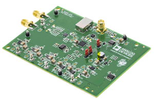
Analog Devices Inc.The AD9856 integrates a high-speed direct-digital synthesizer (DDS), a high-performance, high-speed 12-bit Digital-to-Analog converter (DAC), clock multiplier circuitry, digital filters, and other DSP functions onto a single chip, to form a complete quadrature digital upconverter device. The AD9856 is primarily intended to function as a universal upstream and downstream I/Q modulator for interactive HFC cable network applications, where cost, size, power dissipation, and dynamic performance are critical attributes.
ADA4412-3ARQZ-R7
Part Number : ADA4412-3ARQZ-R7
Analog Devices Inc.The ADA4412-3 is a comprehensive filtering solution designed to give designers the flexibility to easily filter and drive various video signals, including high definition video. Cutoff frequencies of the 6th order video filters range from 9 MHz to 36 MHz. The filters are tuned for RGB, high definition, and standard definition video signals.The ADA4412-3 includes an output offset voltage adjustment feature. Output voltage offset is continuously adjustable over an input-referred range of ±500 mV by applying a differential voltage to an independent offset control input.The ADA4412-3 can operate on a single +5 V supply as well as ±5 V supplies. Single-supply operation is ideal in applications where power consumption is critical. The disable feature allows for further power conservation by greatly reducing the supply current when a particular device is not in use.The ADA4412-3 is available in the 20-lead QSOP package and is rated for operation over the industrial temperature range of -40°C to +85°C.APPLICATIONS Set-top boxes DVD players and recorders Personal video recorders HDTVs Projectors
ADCMP371AKSZ-REEL7
Part Number : ADCMP371AKSZ-REEL7
Analog Devices Inc.The ADCMP370 / ADCMP371 are general-purpose comparators with input offset voltages of 9 mV (max) and low power consumption, which make them ideal for battery-powered portable equipment.The ADCMP371 has a push-pull output stage, while the ADCMP370 has an open-drain output. The inputs on both parts and the output on the ADCMP370 can tolerate voltages up to 22 V, making them suitable for use as voltage detectors in portable equipment.They are available in space-efficient 5-lead SC70 packaging.APPLICATIONS Battery Management Systems A/D Converters Low Voltage Applications Battery Powered Electronics Portable Equipment
ADCMP563BRQZ
Part Number : ADCMP563BRQZ
Analog Devices Inc.The ADCMP563/ADCMP564 are high speed comparatorsfabricated on Analog Devices’ proprietary XFCB process. Thedevices feature a 700 ps propagation delay with less than 75 psoverdrive dispersion. Dispersion, a measure of the difference inpropagation delay under differing overdrive conditions, is a particularlyimportant characteristic of high speed comparators. A separateprogrammable hysteresis pin is available on the ADCMP564.A differential input stage permits consistent propagation delaywith a wide variety of signals in the common-mode range from−2.0 V to +3.0 V. Outputs are complementary digital signals thatare fully compatible with ECL 10 K and 10 KH logic families.The outputs provide sufficient drive current to directly drivetransmission lines terminated in 50 Ω to −2 V. A latch input,which is included, permits tracking, track-and-hold, or sample-and-holdmodes of operation. The latch input pins contain internalpull-ups that set the latch in tracking mode when left open.The ADCMP563/ADCMP564 are specified over the industrialtemperature range (−40°C to +85°C).Applications Automatic test equipment High speed instrumentation Scope and logic analyzer front ends Window comparators High speed line receivers Threshold detection Peak detection High speed triggers Patient diagnostics Hand-held test instruments Zero crossing detectors Line receivers and signal restoration Clock drivers
EV-ADF4360-2EB1Z
Part Number : EV-ADF4360-2EB1Z
Analog Devices Inc.The ADF4360-2 is a fully integrated integer-N synthesizerand voltage-controlled oscillator (VCO). The ADF4360-2 isdesigned for a center frequency of 2000 MHz. In addition, adivide-by-2 option is available, whereby the user gets an RFoutput of between 925 MHz and 1085 MHz.Control of all the on-chip registers is through a simple 3-wireinterface. The device operates with a power supply rangingfrom 3.0 V to 3.6 V and can be powered down when not in use.Applications Wireless handsets (DECT, GSM, PCS, DCS, WCDMA) Test equipment Wireless LANs CATV equipment
EVAL-AD5235SDZ
Part Number : EVAL-AD5235SDZ
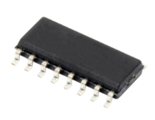
Analog Devices Inc.The AD5235 is a dual-channel, nonvolatile memory, digitallycontrolled potentiometer with 1024-step resolution, offeringguaranteed maximum low resistor tolerance error of ±8%.The device performs the same electronic adjustment functionas a mechanical potentiometer with enhanced resolution, solidstate reliability, and superior low temperature coefficient performance.The versatile programming of the AD5235 via anSPI®-compatible serial interface allows 16 modes of operationand adjustment including scratchpad programming, memorystoring and restoring, increment/decrement, ±6 dB/step log taperadjustment, wiper setting readback, and extra EEMEM for user-definedinformation such as memory data for other components,look-up table, or system identification information.In the scratchpad programming mode, a specific setting canbe programmed directly to the RDAC register, which sets theresistance between Terminal W and Terminal A and Terminal Wand Terminal B. This setting can be stored into the EEMEMand is restored automatically to the RDAC register duringsystem power-on.The EEMEM content can be restored dynamically or throughexternal PR strobing, and a WP function protects EEMEMcontents. To simplify the programming, the independent orsimultaneous linear-step increment or decrement commandscan be used to move the RDAC wiper up or down, one step ata time. For logarithmic ±6 dB changes in the wiper setting, theleft or right bit shift command can be used to double or halve theRDAC wiper setting.The AD5235 patterned resistance tolerance is stored in theEEMEM. The actual end-to-end resistance can, therefore, beknown by the host processor in readback mode. The host canexecute the appropriate resistance step through a softwareroutine that simplifies open-loop applications as well asprecision calibration and tolerance matching applications.The AD5235 is available in a thin, 16-lead TSSOP package.The part is guaranteed to operate over the extended industrialtemperature range of −40°C to +85°C.Applications DWDM laser diode driver, optical supervisory systems Mechanical potentiometer replacement Instrumentation: gain, offset adjustment Programmable voltage-to-current conversion Programmable filters, delays, time constants Programmable power supply Low resolution DAC replacement Sensor calibration
ADM485ARMZ
Part Number : ADM485ARMZ
Analog Devices Inc.The ADM485 is a differential line transceiver suitable for high speed bidirectional data communication on multipoint bus transmission lines. It is designed for balanced data transmission and complies with both EIA Standards RS-485 and RS-422. The part contains a differential line driver and a differential line receiver. Both the driver and the receiver may be enabled independently. When disabled, the outputs are tristated.The ADM485 operates from a single +5 V power supply. Excessive power dissipation caused by bus contention or by output shorting is prevented by a thermal shutdown circuit. This feature forces the driver output into a high impedance state if during fault conditions a significant temperature increase is detected in the internal driver circuitry.Up to 32 transceivers may be connected simultaneously on a bus, but only one driver should be enabled at any time. It is important, therefore, that the remaining disabled drivers do not load the bus. To ensure this, the ADM485 driver features high output impedance when disabled and also when powered down. This minimizes the loading effect when the transceiver is not being utilized. The high impedance driver output is maintained over the entire common-mode voltage range form -7V to +12 V.The receiver contains a fail safe feature which results in a logic high output state if the inputs are unconnected (floating).The ADM485 is fabricated on BiCMOS, an advanced mixed technology process combining low power CMOS with fast switching bipolar technology. All inputs and outputs contain protection against EDS; all diver outputs feature high source and sink current capability. An epitaxial layer is used to guard against latch-up.The ADM485 features extremely fast switching speeds. Minimal driver propagation delays permit transmission at data rates up to 5 Mbits/s while low skew minimizes EMI interference. The part is fully specified over the commercial and industrial temperature range and is available in an 8-pin DIL/SOIC packages.
ADUC843BCP32Z-5
Part Number : ADUC843BCP32Z-5
Analog Devices Inc.The ADuC841/ADuC842/ADuC843 are complete smart transducer front ends, that integrates a high performance self-calibrating multichannel ADC, a dual DAC, and an optimized single-cycle 20 MHz 8-bit MCU (8051 instruction set compatible) on a single chip.The ADuC841 and ADuC842 are identical with the exception of the clock oscillator circuit; the ADuC841 is clocked directly from an external crystal up to 20 MHz whereas the ADuC842 uses a 32 kHz crystal with an on-chip PLL generating a programmable core clock up to 16.78 MHz.The ADuC843 is identical to the ADuC842 except that the ADuC843 has no analog DAC outputs.The microcontroller is an optimized 8052 core offering up to 20 MIPS peak performance. Three different memory options are available offering up to 62 kBytes of nonvolatile Flash/EE program memory. Four kBytes of nonvolatile Flash/EE data memory, 256 bytes RAM, and 2 kBytes of extended RAM are also integrated on-chip. The parts also incorporate additional analog functionality with two 12-bit DACs, power supply monitor, and a band gap reference. On-chip digital peripherals include two 16-bit Σ-Δ. DACs, a dual output 16-bit PWM, a watchdog timer, a time interval counter, three timers/counters, and three serial I/O ports (SPI, I2C, and UART).On the ADuC812 and the ADuC832, the I2C and SPI interfaces share some of the same pins. For backwards compatibility, this is also the case for the ADuC841/ADuC842/ADuC843.However, there is also the option to allow SPI operate separately on P3.3, P3.4, and P3.5, while I2C uses the standard pins. The I2C interface has also been enhanced to offer repeated start, general call, and quad addressing.On-chip factory firmware supports in-circuit serial download and debug modes (via UART) as well as single-pin emulation mode via the EA pin.Applications Optical networking—laser power control Base station systems Precision instrumentation, smart sensors Transient capture systems DAS and communications systems
ADUC843BCPZ32-3
Part Number : ADUC843BCPZ32-3
Analog Devices Inc.The ADuC841/ADuC842/ADuC843 are complete smart transducer front ends, that integrates a high performance self-calibrating multichannel ADC, a dual DAC, and an optimized single-cycle 20 MHz 8-bit MCU (8051 instruction set compatible) on a single chip.The ADuC841 and ADuC842 are identical with the exception of the clock oscillator circuit; the ADuC841 is clocked directly from an external crystal up to 20 MHz whereas the ADuC842 uses a 32 kHz crystal with an on-chip PLL generating a programmable core clock up to 16.78 MHz.The ADuC843 is identical to the ADuC842 except that the ADuC843 has no analog DAC outputs.The microcontroller is an optimized 8052 core offering up to 20 MIPS peak performance. Three different memory options are available offering up to 62 kBytes of nonvolatile Flash/EE program memory. Four kBytes of nonvolatile Flash/EE data memory, 256 bytes RAM, and 2 kBytes of extended RAM are also integrated on-chip. The parts also incorporate additional analog functionality with two 12-bit DACs, power supply monitor, and a band gap reference. On-chip digital peripherals include two 16-bit Σ-Δ. DACs, a dual output 16-bit PWM, a watchdog timer, a time interval counter, three timers/counters, and three serial I/O ports (SPI, I2C, and UART).On the ADuC812 and the ADuC832, the I2C and SPI interfaces share some of the same pins. For backwards compatibility, this is also the case for the ADuC841/ADuC842/ADuC843.However, there is also the option to allow SPI operate separately on P3.3, P3.4, and P3.5, while I2C uses the standard pins. The I2C interface has also been enhanced to offer repeated start, general call, and quad addressing.On-chip factory firmware supports in-circuit serial download and debug modes (via UART) as well as single-pin emulation mode via the EA pin.Applications Optical networking—laser power control Base station systems Precision instrumentation, smart sensors Transient capture systems DAS and communications systems
DAC8228FPZ
Part Number : DAC8228FPZ
Analog Devices Inc.The DAC-8228 is a dual 8-bit, voltage output, CMOS, D/A converter in a single chip. It was designed to drop into AD7528 / AD7628 sockets eliminating two external op amps in applications such as hard diskdrives. These applications generally operate the AD7528 / AD7628 with zero volts applied to VREF and offset AGND to +2.5 or +5 volts. The DAC-8228 is tested under both these conditions.The DAC-8228 can also be used in those applications requiring a unipolar output voltage. It can deliver an output voltage between 0V and +10V with VDD = +14V (maximum output voltage is VDD -4V). The DAC-8228's reference input can accept a negative voltage from 0V to -10V (the DAC's internal unity-gain inverting amplifier inverts the input signal). Choose the DAC-8229 for bipolar operation.The DAC8228 offers CerDIP and plastic packaged devices in the extended industrial temperature range of -40° to +85°C. Applications requiring the military temperature range should use the DAC-8229. To make the DAC-8229 pin and functionally compatible with the DAC-8228, AGND A and AGND B should be tied together to function as VZ, and VSS connected to GND.The DAC-8228 consists of two CMOS voltage output amplifiers, two high-accuracy R-2R resistor ladder networks, interface control logic, and two 8-bit registers. An internal regulator maintains TTL logic compatibility and fast microprocessor interface timing over the full VDD range.The DAC-8228 dissipates only 90mW in the space saving 20-pin 0.3' DIP or the 20-lead SO surface mount package. Its compact size, low power, and economical cost per channel, makes it attractive for applications requiring multiple D/A converters without sacrificing circuit-board space. Reduced parts count also improves system reliability.Using PMI's advanced oxide-isolated, silicon-gate CMOS process, coupled with its highly-stable thin-film resistor ladder, allows the DAC-8228 to offer superior matching and temperature tracking between DACs.APPLICATIONS Disk Drive Systems Automatic Test Equipment Process/Industrial Controls Energy Controls Programmable Instrumentation Multi-Channel Microprocessor-Controlled Systems Servo Control Systems
DC817A
Part Number : DC817A
Analog Devices Inc.The LTC2927 provides a simple solution to power supply tracking and sequencing requirements. By selecting a few resistors, the supply can be configured to ramp-up and ramp-down with differing ramp rates, voltage offsets, or time delays relative to other supplies or a master signal.By forcing current into a feedback node of an independent supply, the LTC2927 causes the output to track a ramp signal without inserting any pass element losses. Because the current is controlled in an open-loop manner, the LTC2927 does not affect the transient response or stability of the supply. The compact solution at point of load minimizes the trace length of the DC/DC circuit sensitive FB node. Furthermore, it presents a high impedance when power-up is complete, effectively removing it from the DC/DC circuit.Applications VCORE and VI/O Supply Tracking Microprocessor, DSP and FPGA Supplies Multiple Supply Systems Point-of-Load Supplies
REF198ESZ-REEL7
Part Number : REF198ESZ-REEL7
Analog Devices Inc.The REF19x series precision band gap voltage references use a patented temperature drift curvature correction circuit and laser trimming of highly stable, thin-film resistors to achieve a very low temperature coefficient and high initial accuracy.The REF19x series is made up of micropower, low dropout voltage (LDV) devices, providing stable output voltage from supplies as low as 100 mV above the output voltage and consuming less than 45 μA of supply current. In sleep mode, which is enabled by applying a low TTL or CMOS level to the SLEEP pin, the output is turned off and supply current is further reduced to less than 15 μA.The REF19x series references are specified over the extended industrial temperature range (−40°C to +85°C) with typical performance specifications over −40°C to +125°C for applications, such as automotive.All electrical grades are available in an 8-lead SOIC package; the PDIP and TSSOP packages are available only in the lowest electrical grade.APPLICATIONS Portable instruments ADCs and DACs Smart sensors Solar powered applications Loop-current-powered instruments
SSM2141PZ
Part Number : SSM2141PZ
Analog Devices Inc.The SSM2141 is an integrated differential amplifier intended to receive balanced line inputs in audio applications requiring a high level of noise immunity and optimum common-mode rejection. The SSM2141 typically achieves 100 dB of common-mode rejection (CMR), whereas implementing an op amp with four off-the-shelf precision resistors will typically achieve only 40 dB of CMR-inadequate for high-performance audio.The SSM2141 achieves low distortion performance by maintaining a large slew rate of 9.5 V/µs and high open-loop gain. Distortion is less than 0.002% over the full audio bandwidth. The SSM2141 complements the SSM2142 balanced line driver. Together, these devices comprise a fully integrated solution for equivalent transformer balancing of audio signals without the problems of distortion, EMI fields, and high cost.Additional applications for the SSM2141 include summing signals, differential preamplifiers, and 600 Ohm low distortion buffer amplifiers. For similar performance with G = 1/2, see SSM2143.APPLICATIONS Line Receivers Summing Amplifiers Buffer Amplifiers–Drives 600 Ω Load
SSM2141SZ
Part Number : SSM2141SZ
Analog Devices Inc.The SSM2141 is an integrated differential amplifier intended to receive balanced line inputs in audio applications requiring a high level of noise immunity and optimum common-mode rejection. The SSM2141 typically achieves 100 dB of common-mode rejection (CMR), whereas implementing an op amp with four off-the-shelf precision resistors will typically achieve only 40 dB of CMR-inadequate for high-performance audio.The SSM2141 achieves low distortion performance by maintaining a large slew rate of 9.5 V/µs and high open-loop gain. Distortion is less than 0.002% over the full audio bandwidth. The SSM2141 complements the SSM2142 balanced line driver. Together, these devices comprise a fully integrated solution for equivalent transformer balancing of audio signals without the problems of distortion, EMI fields, and high cost.Additional applications for the SSM2141 include summing signals, differential preamplifiers, and 600 Ohm low distortion buffer amplifiers. For similar performance with G = 1/2, see SSM2143.APPLICATIONS Line Receivers Summing Amplifiers Buffer Amplifiers–Drives 600 Ω Load
SSM2143PZ
Part Number : SSM2143PZ
Analog Devices Inc.The SSM2143 is an integrated differential amplifier intended to receive balanced line inputs in audio applications requiring a high level of immunity from common-mode noise. The device provides a typical 90 dB of common-mode rejection (CMR), which is achieved by laser trimming of resistances to better than 0.005%.Additional features of the device include a slew rate of 10 V/µs and wide bandwidth. Total harmonic distortion (THD) is less than 0.004% over the full audio band, even while driving low impedance loads. The SSM2143 input stage is designed to handle input signals as large as +28 dBu at G = 1/2. Although primarily intended for G = 1/2 applications, a gain of 2 can be realized by reversing the +IN/-IN and SENSE/REFERENCE connections.When configured for a gain of 1/2, the SSM2143 and SSM2142 Balanced Line Driver provide a fully integrated, unity gain solution to driving audio signals over long cable runs. For similar performance with G = 1, see SSM2141.
ADSP-21364YSWZ-2AA
Part Number : ADSP-21364YSWZ-2AA
Analog Devices Inc.The ADSP-2136x SHARC® processor is a member of the SIMD SHARC family of DSPs that feature Analog Devices, Inc., Super Harvard Architecture. The processor is source code-compatible with the ADSP-2126x and ADSP-2116x DSPs, as well as with first generation ADSP-2106x SHARC processors in SISD (single-instruction, single-data) mode. The ADSP-2136x are 32-/40-bit floating-point processors optimized for high performance automotive audio applications. They contain a large on-chip SRAM and ROM, multiple internal buses to eliminate I/O bottlenecks, and an innovative digital audio interface (DAI).As shown in the functional block diagram on Page 1, the ADSP-2136x uses two computational units to deliver a significant performance increase over the previous SHARC processors on a range of signal processing algorithms. With its SIMD computational hardware, the ADSP-2136x can perform two GFLOPS running at 333 MHz.
ADSP-BF525ABCZ-6
Part Number : ADSP-BF525ABCZ-6
Analog Devices Inc.The ADSP-BF525 offers up to 600 MHz performance and up to 1200 MMACs. This processor core is supported by an advanced DMA controller supporting one-and two-dimensional DMA transfers between on-chip memory, off-chip memory, and system peripherals. The combination of the processor core speed and the DMA controller allows for efficient processing of audio, voice, video, and image data.The ADSP-BF525 provides peripheral flexibility to complement its high performance processing. The HS USB OTG host direct memory access (HDMA) and NAND flash controller are just a few of the peripheral options on the ADSP-BF525 family—not to mention the availability of up to 48 GPIO ports.For applications where product differentiation represents a challenge for securing market leadership, the ADSP-BF525 enables developers to provide features and benefits to augment their product offerings without compromising cost or power. The scalability of the ADSP-BF525 makes it an ideal candidate for Premium Audio Players where differentiation of features can be realized without sacrificing system cost. Where the diversity of Multimedia applications and content security are key attributes the ADSP-BF525 provides processing flexibility and Lockbox™ Secure Technology to enable users to develop freely and without bounds.IP protection has become a necessary part of today’s embedded computing applications. The ADSP-BF525 provides a security scheme which balances flexibility and upgradeability with performance through the inclusion of a firmware-based solution including OTP (One Time Programmable) memory to enable users to implement private keys for secure access to program code.
ADSP-BF527BBCZ-5A
Part Number : ADSP-BF527BBCZ-5A
Analog Devices Inc.The high performance 16/32-bit Blackfin embedded processor core, the flexible cache architecture, the enhanced DMA subsystem, and the dynamic power management (DPM) functionality allow system designers a flexible platform to address a wide range of portable applications, including consumer, communications and industrial/instrumentation.With the combination of peripherals which enable glue-less connectivity to networked devices such as Ethernet or WiFi 802.11 a/b/g modules and power efficient signal processing, the ADSP-BF527 is well suited to IP connected applications such as VoIP Phone or IP Camera.The VoIP challenge to the embedded-system designer is to choose a processing solution that is cost-effective, easy to deploy and scaleable in performance across market spaces. A “sweet spot” embedded-solution approach is to design with a platform that can implement a low channel count basic VoIP solution, yet retain sufficient capacity for value added capabilities and services – such as video, music, imaging and system control. Unlike traditional VoIP embedded solutions that utilize two processor cores to provide VoIP functionality, the ADSP-BF527 provides a convergent solution in a unified core architecture that allows voice and video signal processing concurrent with RISC MCU processing to handle network and user-interface demands. This unique ability to offer full VoIP functionality on a single convergent processor provides for a unified software development environment, faster system debugging and deployment, and lower overall system cost.IP protection has become a necessary part of today’s embedded computing applications. The ADSP-BF527 provides a security scheme which balances flexibility and upgradeability with performance through the inclusion of a firmware-based solution including OTP (One Time Programmable) memory to enable users to implement private keys for secure access to program code.
ADSP-BF532SBSTZ400
Part Number : ADSP-BF532SBSTZ400
Analog Devices Inc.The ADSP-BF531 / ADSP-BF532 / ADSP-BF533 processors are members of the Blackfin® family of products, incorporating the Analog Devices, Inc./Intel Micro Signal Architecture (MSA). Blackfin processors combine a dual-MAC state-of-the-art signal processing engine, the advantages of a clean, orthogonal RISC-like microprocessor instruction set, and single instruction, multiple data (SIMD) multimedia capabilities into a single instruction set architecture. The ADSP-BF531 / ADSP-BF532 / ADSP-BF533 processors are completely code and pin-compatible, differing only with respect to their performance and on-chip memory. Specific performance and memory configurations are shown in Table 1.PERIPHERALS Parallel peripheral interface PPI, supporting ITU-R 656 video data formats 2 dual-channel, full duplex synchronous serial ports, supporting eight stereo I2S channels 2 memory-to-memory DMAs 8 peripheral DMAs SPI-compatible port Three 32-bit timer/counters with PWM support Real-time clock and watchdog timer 32-bit core timer Up to 16 general-purpose I/O pins (GPIO) UART with support for IrDA Event handler Debug/JTAG interface On-chip PLL capable of frequency multiplication
ADSP-BF561SKBCZ-5A
Part Number : ADSP-BF561SKBCZ-5A
Analog Devices Inc.The Blackfin® Processor family expands the performance envelope with the ADSP-BF561. With two high performance Blackfin Processor cores, flexible cache architecture, enhanced DMA subsystem, and Dynamic Power Management (DPM) functionality, the ADSP-BF561 can support complex control and signal processing tasks while maintaining extremely high datathroughput.The ADSP-BF561 is a functional extension of the popular Blackfin Processor family and is ideally suited for a broad range of industrial, instrumentation, medical, and consumer appliance applications—allowing for scalability based upon the required data bandwidth and mix of control, plus signal processing needed in the end product.High-Level of Integration 328 KBytes of on-chip memory configured as: 32 KBytes of L1 instruction memory SRAM/Cache per core 64 KBytes of L1 data memory SRAM/Cache per core 4 KBytes of L1 scratchpad memory per core 128 KBytes of low-latency shared L2 memory 32-bit Memory Controller providing glueless connection to multiple banks of SDRAM, SRAM, Flash or ROM. Two Parallel Peripheral Interfaces Units supporting ITU-R 656 video data formats. Two dual-channel, full-duplex, synchronous serial ports supporting eight stereo I2S channels. Dual 16 Channel DMA Controllers, supporting one and two-dimension transfers. SPI-compatible Port. UART with support for IrDA®. 12 timer/counters supporting PWM, pulsewidth and event count modes. 48 Programmable Flags/General Purpose I/O. Event Handler. Dual Watchdog timers. PLL capable of 1x to 63x frequency multiplication. 256-ball Mini-BGA and 297-ball Sparse PBGA packages.


