ADUM2251ARWZ
Part Number : ADUM2251ARWZ
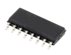
Analog Devices Inc.The ADuM2250 / ADuM2251 are hot swappable digital isolators with non-latching, bidirectional communication channels and are compatible with I2C interfaces. This eliminates the need for splitting I2C signals into separate transmit and receive signals for use with stand-alone optocouplers.The ADuM2250 provides two bidirectional channels, supporting a complete isolated I2C interface. The ADuM2251 provides one bidirectional channel and one unidirectional channel for those applications where a bidirectional clock is not required.The ADuM2250 / ADuM2251 contain hot swap circuitry to prevent data glitches when an unpowered card is inserted onto an active bus.These isolators are based on iCoupler® chip scale transformer technology from Analog Devices, Inc. iCoupler is a magnetic isolation technology with functional, performance, size, and power consumption advantages compared to optocouplers. The ADuM2250 / ADuM2251 integrate iCoupler channels with semiconductor circuitry to enable a complete, isolated I2C interface provided in a small form factor.APPLICATIONS Isolated I2C, SMbus, or PMBus Interfaces Multilevel I2C interfaces Power supplies Networking Power over Ethernet
ADUM2251WARWZ
Part Number : ADUM2251WARWZ
Analog Devices Inc.The ADuM2250 / ADuM2251 are hot swappable digital isolators with non-latching, bidirectional communication channels and are compatible with I2C interfaces. This eliminates the need for splitting I2C signals into separate transmit and receive signals for use with stand-alone optocouplers.The ADuM2250 provides two bidirectional channels, supporting a complete isolated I2C interface. The ADuM2251 provides one bidirectional channel and one unidirectional channel for those applications where a bidirectional clock is not required.The ADuM2250 / ADuM2251 contain hot swap circuitry to prevent data glitches when an unpowered card is inserted onto an active bus.These isolators are based on iCoupler® chip scale transformer technology from Analog Devices, Inc. iCoupler is a magnetic isolation technology with functional, performance, size, and power consumption advantages compared to optocouplers. The ADuM2250 / ADuM2251 integrate iCoupler channels with semiconductor circuitry to enable a complete, isolated I2C interface provided in a small form factor.APPLICATIONS Isolated I2C, SMbus, or PMBus Interfaces Multilevel I2C interfaces Power supplies Networking Power over Ethernet
ADV7180BCP32Z
Part Number : ADV7180BCP32Z
Analog Devices Inc.The ADV7180 automatically detects and converts standard analog baseband television signals compatible with worldwide NTSC, PAL, and SECAM standards into 4:2:2 component video data compatible with the 8-bit ITU-R BT.656 interface standard.The simple digital output interface connects gluelessly to a wide range of MPEG encoders, codecs, mobile video processors, and Analog Devices, Inc., digital video encoders, such as the ADV7391. External HS, VS, and FIELD signals provide timing references for LCD controllers and other video ASICs, if required. Accurate 10-bit analog-to-digital conversion provides professional quality video performance for consumer applications with true 8-bit data resolution. Three analog video input channels accept standard composite, S-video, or component video signals, supporting a wide range of consumer video sources. AGC and clamp-restore circuitry allow an input video signal peak-to-peak range to 1.0 V. Alternatively, these can be bypassed for manual settings.The line-locked clock output allows the output data rate, timing signals, and output clock signals to be synchronous, asynchronous, or line locked even with ±5% line length variation. Output control signals allow glueless interface connections in many applications. The ADV7180 is programmed via a 2-wire, serial bidirectional port (I2C® compatible) and is fabricated in a 1.8 V CMOS process. Its monolithic CMOS construction ensures greater functionality with lower power dissipation. LFCSP package options makes the decoder ideal for space-constrained portable applications. A 64-lead LQFP package is pin compatible with the ADV7181C.The 48-Lead LQFP, 40-lead LFCSP, and 32-lead LFCSP use one pin to output VS or FIELD.APPLICATIONS Digital camcorders and PDAs Low cost SDTV PIP decoder for digital TVs Multichannel DVRs for video security AV receivers and video transcoding PCI-/USB-based video capture and TV tuner cards Personal media players and recorders Smartphone/multimedia handsets In-car/automotive infotainment units Rearview camera/vehicle safety systems
ADV7800BSTZ-150
Part Number : ADV7800BSTZ-150
Analog Devices Inc.The ADV7800 is a high quality, single-chip, multiformat 3D comb filter, video decoder, and graphics digitizer. This multiformat 3D comb filter decoder supports the conversion of PAL, NTSC, and SECAM standards in the form of a composite or an S-Video into a digital ITU-R BT.656 format. The ADV7800 also supports the decoding of a component RGB/YPbPr video signal into a digital YCrCb or RGB pixel output stream.The support for component video includes standards such as 525i, 625i, 525p, 625p, 720p, 1080i, 1080p, and many other HD and SMPTE standards. Graphics digitization is supported by the ADV7800; it is capable of digitizing RGB graphics signals from VGA to SXGA rates and converting them into a digital RGB or YCrCb pixel output stream. SCART and overlay functionality are enabled by the ability of the ADV7800 to simultaneously process CVBS and standard definition RGB signals.The ADV7800 contains two main processing sections. The first section is the standard definition processor (SDP), which processes all PAL, NTSC, SECAM, and component (up to 525p/625p) signal types. The second section is the component processor (CP), which processes YPrPb and RGB component formats, including RGB graphics.APPLICATIONS AV receiver LCD HDTVs PDP HDTVs CRT HDTVs HDTV STBs with PVR DVD recorders with progressive scan input support
ADXL203CE
Part Number : ADXL203CE
Analog Devices Inc.The ADXL203 is a high precision, low power, complete dual-axis accelerometer with signal conditioned voltage outputs, all on a single, monolithic IC. The ADXL203 measures acceleration with a full-scale range of ±1.7 g, ±5 g, or ±18 g. The ADXL203 can measure both dynamic acceleration (for example, vibration) and static acceleration (for example, gravity).The typical noise floor is 110 μg/√Hz, allowing signals below 1 mg (0.06° of inclination) to be resolved in tilt sensing applications using narrow bandwidths (
DAC8413FPCZ
Part Number : DAC8413FPCZ
Analog Devices Inc.The DAC8412 / DAC8413 are quad, 12-bit voltage output DACs with readback capability. Built using a complementary BiCMOS process, these monolithic DACs offer the user very high package density.Output voltage swing is set by the two reference inputs VREFH and VREFL. By setting the VREFL input to 0 V and VREFH to a positive voltage, the DAC provides a unipolar positive output range. A similar configuration with VREFH at 0 V and VREFL at a negative voltage provides a unipolar negative output range. Bipolar outputs are configured by connecting both VREFH and VREFL to nonzero voltages. This method of setting output voltage range has advantages over other bipolar offsetting methods because it is not dependent on internal and external resistors with different temperature coefficients.Digital controls allow the user to load or read back data from any DAC, load any DAC, and transfer data to all DACs at one time.An active low RESET loads all DAC output registers to midscale for the DAC8412 and zero scale for the DAC8413.The DAC8412 / DAC8413 are available in 28-lead plastic DIP, 28-lead ceramic DIP, 28-lead PLCC, and 28-lead LCC packages.They can be operated from a wide variety of supply and reference voltages with supplies ranging from single +5 V to ±15 V, and references from +2.5 V to ±10 V. Power dissipation is less than 330 mW with ±15 V supplies and only 60 mW with a +5 V supply.For MIL-STD-883 applications, contact your local Analog Devices, Inc. sales office for the DAC8412/DAC8413/883 data sheet, which specifies operation over the −55°C to +125°C temperature range. All 883 parts are also available on Standard Military Drawings 5962-91 76401MXA through 76404M3A.APPLICATIONS Automatic test equipment Digitally controlled calibration Servo controls Process control equipment
DC1099A
Part Number : DC1099A
Analog Devices Inc.The LTC2953 is a push button On/Off controller that manages system power via a push button interface. An enable output toggles system power while an interrupt output provides debounced push button status. The interrupt output can be used in menu driven applications to request a system power down. The LTC2953 also features input and output power supply monitors. An uncommitted power fail comparator provides real time input monitor information, while a de-glitched under voltage lockout comparator gracefully initiates a system power down. The under voltage lockout comparator prevents the system from powering from a low power supply. The adjustable supply monitor input is compared against an accurate internal 0.5V reference. The reset output remains low until the supply monitor input has been in compliance for 200ms. The LTC2953 operates over a wide 2.7V to 27V input voltage range and draws only 14µA of current. Two versions of the part accommodate either positive or negative enable polarities. Applications Push Button Power Path Control Battery Power Supervisor Portable Instrumentation, PDA Blade Servers Desktop and Notebook Computers
DC1195A
Part Number : DC1195A
Analog Devices Inc.The LTM8023 is a complete 2A, DC/DC step-down power supply. Included in the package are the switching controller, power switches, inductor, and all support components. Operating over an input voltage range of 3.6V to 36V, the LTM8023 supports an output voltage range of 0.8V to 10V, and a switching frequency range of 200kHz to 2.4MHz, each set by a single resistor. Only the bulk input and output filter capacitors are needed to finish the design.The low profile package enables utilization of unused space on the bottom of PC boards for high density point of load regulation.The LTM8023 is packaged in a thermally enhanced, compact and low profile over-molded land grid array (LGA) and ball grid array (BGA) packages suitable for automated assembly by standard surface mount equipment. The LTM8023 is available with SnPb (BGA) or RoHS compliant terminal finish.Applications Automotive Battery Regulation Power for Portable Products Distributed Supply Regulation Industrial Supplies Wall Transformer Regulation
EVAL-AD2S1205SDZ
Part Number : EVAL-AD2S1205SDZ
Analog Devices Inc.The AD2S1205 is a complete 12-bit resolution tracking resolver-to-digital converter that contains an on-board programmable sinusoidal oscillator providing sine wave excitation for resolvers.The converter accepts 3.15 VP-P ± 27% input signals on the Sin and Cos inputs. A Type II tracking loop is employed to track the inputs and convert the input Sin and Cos information into a digital representation of the input angle and velocity. The maximum tracking rate is a function of the external clock frequency. The performance of the AD2S105 is specified across a frequency range of 8.192 MHz ± 25%, allowing a maximum tracking rate of 1250 rps.PRODUCT HIGHLIGHTS Ratiometric Tracking Conversion. The Type II tracking loop provides continuous output position data without conversion delay. It also provides noise immunity and tolerance of harmonic distortion on the reference and input signals. System Fault Detection. A fault detection circuit can sense loss of resolver signals, out-of-range input signals, input signal mismatch, or loss of position tracking. Input Signal Range. The Sin and Cos inputs can accept differential input voltages of 3.15 VP-P ± 27%. Programmable Excitation Frequency. Excitation frequency is easily programmable to 10 kHz, 12 kHz, 15 kHz, or 20 kHz by using the frequency select pins (the FS1 and FS2 pins). Triple Format Position Data. Absolute 12-bit angular position data is accessed via either a 12-bit parallel port or a 3-wire serial interface. Incremental encoder emulation is in standard A-quad-B format with direction output available. Digital Velocity Output. 12-bit signed digital velocity accessed via either a 12-bit parallel port or a 3-wire serial interface. APPLICATIONS Automotive motion sensing and control Hybrid-electric vehicles Electric power steering Integrated starter generator/alternator Industrial motor control Process control
EVAL-ADF7021DBZ2
Part Number : EVAL-ADF7021DBZ2
Analog Devices Inc.The ADF7021 is a low power, highly integrated 2FSK/3FSK/4FSK transceiver. It is designed to operate in the narrowband, license-free ISM bands and licensed bands in the 80 MHz to 650 MHz and 862 MHz to 940 MHz frequency ranges. It has both Gaussian and raised cosine data filtering options to improve spectral efficiency for narrowband applications.It is suitable for circuit applications targeted at European ETSI-EN 300-220, the Japanese ARIB STD-T67, the Chinese Short Range Device regulations, and the North American FCC Part 15, Part 90, and Part 95 regulatory standards. A complete transceiver can be built using a small number of external discrete components, making the ADF7021 very suitable for price-sensitive and area-sensitive applications.The transmit section contains a voltage controlled oscillator (VCO) and a low noise fractional-N PLL with output resolution of
EVAL-ADF7021DBZ3
Part Number : EVAL-ADF7021DBZ3
Analog Devices Inc.The ADF7021 is a low power, highly integrated 2FSK/3FSK/4FSK transceiver. It is designed to operate in the narrowband, license-free ISM bands and licensed bands in the 80 MHz to 650 MHz and 862 MHz to 940 MHz frequency ranges. It has both Gaussian and raised cosine data filtering options to improve spectral efficiency for narrowband applications.It is suitable for circuit applications targeted at European ETSI-EN 300-220, the Japanese ARIB STD-T67, the Chinese Short Range Device regulations, and the North American FCC Part 15, Part 90, and Part 95 regulatory standards. A complete transceiver can be built using a small number of external discrete components, making the ADF7021 very suitable for price-sensitive and area-sensitive applications.The transmit section contains a voltage controlled oscillator (VCO) and a low noise fractional-N PLL with output resolution of
EVAL-ADM1186-2MBZ
Part Number : EVAL-ADM1186-2MBZ
Analog Devices Inc.The ADM1186-1 and ADM1186-2 are integrated, four-channel, voltage monitoring and sequencing devices. A 2.7 V to 5.5 V power supply is required on the VCC pin for power.Four precision comparators monitor four voltage rails, with all comparators sharing a 0.6 V reference and a worst-case accuracy of 0.8%. Resistor networks that are external to the VIN1, VIN2, VIN3, and VIN4 pins set the Under Voltage (UV) trip points for the monitored supply rails.The ADM1186-1 and ADM1186-2 have four open drain enable outputs, OUTx, that are used to enable power supplies. An open drain power good output, PWRGD, is provided that indicatesthe four VINx inputs are above their UV thresholds.A state machine monitors the state of the UP and DOWN pins on the ADM1186-1 or the UP/overbar: DOWN pin on the ADM1186-2 to control the supply sequencing direction. In the ‘Wait Start’state, a rising edge transition on the UP or UP/DOWN pin triggers a power-up sequence. A falling edge transition on the DOWN or UP/DOWN pin in the ‘Power Up Done’ statetriggers a power down sequence.During a power up sequence, the state machine enables each power supply in turn. The supply output voltage is monitored to determine if it rises above the UV threshold level within a userdefined duration called the blanking time. If a supply rises above the UV threshold then the next enable output in the sequence is turned on. In addition to the blanking time a user may also define sequencing time delays between each enable output turning on. When all four enable outputs are on, and the four VINx pins are above their UV trip points the power up sequence is complete. The ADM1186-1 provides an open drain pin, SEQ_DONE, that is asserted high to provide an indication that an up sequence is complete. The SEQ_DONE pins is allows multiple cascadedADM1186-1 devices to be perform controlled power up and down sequences. During a power down sequence the enable outputs turn off inreverse order. The sequence time delays between successive supplies the same as during the power up sequence, and no blanking time is used during a power down sequence. At the end of a down sequence the SEQ_DONE pin is brought low. During sequencing and when powered up, the state machine continuously monitors for any fault conditions. Faults include a UV condition on any of the inputs, or an unexpected controlinput. Any fault that occurs causes the state machine to enter a fault handler. This immediately turns off all enable outputs, and ensures that the device is ready to start a new up sequence. The ADM1186-1 has a bi-directional open drain pin, FAULT, that facilitates fault handling when using multiple devices. An ADM1186-1 experiencing a fault condition drives the FAULT pin low, causing other connected ADM1186-1devices to enter their own fault handling state.The ADM1186-1 is available in a 20-lead QSOP package andthe ADM1186-2 is available in a 16-lead QSOP package.
EVAL-ADM1192EBZ
Part Number : EVAL-ADM1192EBZ
Analog Devices Inc.The ADM1192 is an integrated current sense amplifier that offers digital current and voltage monitoring via an on-chip, 12-bit analog-to-digital converter (ADC), communicated through an I2C interface.An internal current sense amplifier senses voltage across the sense resistor in the power path via the VCC pin and the SENSE pin.A 12-bit ADC can measure the current seen in the sense resistor and in the supply voltage on the VCC pin. An industry-standard I2C interface allows a controller to read current and voltage data from the ADC. Measurements can be initiated by an I2C command. Alternatively, the ADC can run continuously, and the user can read the latest conversion data whenever it is required. Up to four unique I2C addresses can be created, depending on the way the ADR pin is connected.A SETV pin is also included. A voltage applied to this pin is internally compared to the output voltage on the current sense amplifier. The output of the SETV comparator asserts when the current sense amplifier output exceeds the SETV voltage. This event is detected at the ALERT block. The ALERT block then charges up the external TIMER capacitor with a fixed current. When this timing cycle is complete, the ALERT output asserts.The ALERT output can be used as a flag to warn a micro-controller or field programmable gate array (FPGA) of an overcurrent condition. ALERT outputs of multiple ADM1192 devices can be tied together and used as a combined alert.A basic P-channel FET hot swap circuit can be implemented with the ALERT output. The value of the TIMER capacitor should be set so that the charging time of this capacitor is much longer than the period where a higher than nominal inrush current may be flowing.The ADM1192 is packaged in a 10-lead MSOP.APPLICATIONS Power monitoring/power budgeting Central office equipment Telecommunication and data communication equipment PCs/servers
LTM4601AHVMPY
Part Number : LTM4601AHVMPY
Analog Devices Inc.The LTM4601AHV is a complete 12A step-down switch mode DC/DC power supply with onboard switching controller, MOSFETs, inductor and all support components. The μModule regulator is housed in a small surface mount 15mm × 15mm × 2.82mm LGA or 15mm × 15mm × 3.42mm BGA package. The LTM4601AHV LGA and BGA packages are designed with redundant mounting pads to enhance solder-joint strength for extended temperature cycling endurance. Operating over an input voltage range of 4.5V to 28V, the LTM4601AHV supports an output voltage range of 0.6V to 5V as well as output voltage tracking and margining. The high efficiency design delivers 12A continuous current (14A peak). Only bulk input and output capacitors are needed to complete the design.The low profile and light weight package easily mounts in unused space on the back side of PC boards for high density point of load regulation. The μModule regulator can be synchronized with an external clock for reducing undesirable frequency harmonics and allows PolyPhase® operation for high load currents.An onboard differential remote sense amplifier can be used to accurately regulate an output voltage independent of load current. The LTM4601AHV is available with SnPb or RoHS compliant terminal finish. LTM4601 LTM4601A LTM4601HV LTM4601AHV Vin Max 20V 20V 28V 28V On Board Remote Sense LTM4601 Yes LTM4601-1 No LTM4601A Yes LTM4601A-1 No Yes Yes Back Side Pads 118 135 (for stronger solder joint stability) 118 135 (for stronger solder joint stability) Applications Telecom, Industrial and Networking Equipment Military and Avionics Systems
REF03GSZ
Part Number : REF03GSZ
Analog Devices Inc.The REF01 / REF02 / REF03 series of precision voltage references provide a stable 10.0 V, 5.0 V, or 2.5 V output with minimal change in response to variations in supply voltage, ambient temperature or load conditions. The devices are available in 8-lead SOIC, PDIP, CERDIP, and TO-99 packages, as well as 20-terminal LCC packages (883 only), furthering the usability of the devices in both standard and high stress applications.With an external buffer and a simple resistor network, the TEMP terminal can be used for temperature sensing and approximation. A TRIM terminal is also provided on the device for fine adjustment of the output voltage.The small footprint, wide supply range, and application versatility make the REF0x series of references ideal for general-purpose and space-constrained applications.Newer designs should use the ADR01 / ADR02 / ADR03 / ADR06 series of references, which offer higher accuracy and temperature stability over a wider operating temperature range, while maintaining full pin-for-pin compatibility with the REF01 / REF02 / REF03 series. This data sheet applies to commercial-grade products only. Contact sales or visit analog.com for military-grade (883) data sheets.APPLICATIONS Precision data systems High resolution converters Industrial process control systems Precision instruments Military and aerospace applications
AD2S90APZ
Part Number : AD2S90APZ
Analog Devices Inc.The AD2S90 is a complete 12-bit resolution tracking resolver-to- digital converter. No external components are required to operate the device.The converter accepts 2 V rms ± 10% input signals in the range 3 kHz-20 kHz on the SIN, COS and REF inputs. A Type II servo loop is employed to track the inputs and convert the input SIN and COS information into a digital representation of the input angle. The bandwidth of the converter is set internally at 1 kHz. The maximum tracking rate is 375 rps at 12-bit resolution.Angular position output information is available in two forms, absolute serial binary and incremental A quad B.The absolute serial binary output is 12-bit (1 in 4096). The data output pin is high impedance when Chip Select CS is logic HI. This allows the connection of multiple converters onto a common bus. Absolute angular information in serial pure binary form is accessed by CS followed by the application of an external clock (SCLK) with a maximum rate of 2 MHz.The encoder emulation outputs A, B and NM continuously produce signals equivalent to a 1024 line encoder.When decoded this corresponds to 12-bits resolution. Three common north marker pulse widths are selected via a single pin (NMC).An analog velocity output signal provides a representation of velocity from a rotating resolver shaft traveling in either a clockwise or counterclockwise direction.The AD2S90 operates on a ±5 V dc ± 5% power supplies and is fabricated on Analog Devices' Linear Compatible CMOS process (LC2MOS). LC2MOS is a mixed technology process that combines precision bipolar circuits with low power CMOS logic circuits.
AD5263BRUZ20
Part Number : AD5263BRUZ20
Analog Devices Inc.The AD5263 is the industry’s first quad-channel, 256-position, digital potentiometer1 with a selectable digital interface. This device performs the same electronic adjustment function as mechanical potentiometers or variable resistors, with enhanced resolution, solid-state reliability, and superior low temperature coefficient performance.Each channel of the AD5263 offers a completely programmable value of resistance between the A terminal and the wiper or between the B terminal and the wiper. The fixed A-to-B terminal resistance of 20 kΩ, 50 kΩ, or 200 kΩ has a nominal temperature coefficient of ±30 ppm/°C and a ±1% channel-to-channel matching tolerance. Another key feature of this part is the ability to operate from +4.5 V to +15 V, or at ±5 V.Wiper position programming presets to midscale upon power-on. Once powered, the VR wiper position is programmed by either the 3-wire SPI or 2-wire I2C-compatible interface. In the I2C mode, additional programmable logic outputs enable users to drive digital loads, logic gates, and analog switches in their systems.The AD5263 is available in a narrow body, 24-lead TSSOP. All parts are guaranteed to operate over the automotive temperature range of –40°C to +125°C.For single- or dual-channel applications, refer to the AD5260 / AD5280 or AD5262 / AD5282 data sheets. APPLICATIONS: Mechanical potentiometer replacement Optical network adjustment Instrumentation: gain, offset adjustment Stereo channel audio level control Automotive electronics adjustment Programmable power supply Programmable filters, delays, time constants Line impedance matching Low resolution DAC/trimmer replacement Base station power amp biasing Sensor calibration
AD5263BRUZ200
Part Number : AD5263BRUZ200
Analog Devices Inc.The AD5263 is the industry’s first quad-channel, 256-position, digital potentiometer1 with a selectable digital interface. This device performs the same electronic adjustment function as mechanical potentiometers or variable resistors, with enhanced resolution, solid-state reliability, and superior low temperature coefficient performance.Each channel of the AD5263 offers a completely programmable value of resistance between the A terminal and the wiper or between the B terminal and the wiper. The fixed A-to-B terminal resistance of 20 kΩ, 50 kΩ, or 200 kΩ has a nominal temperature coefficient of ±30 ppm/°C and a ±1% channel-to-channel matching tolerance. Another key feature of this part is the ability to operate from +4.5 V to +15 V, or at ±5 V.Wiper position programming presets to midscale upon power-on. Once powered, the VR wiper position is programmed by either the 3-wire SPI or 2-wire I2C-compatible interface. In the I2C mode, additional programmable logic outputs enable users to drive digital loads, logic gates, and analog switches in their systems.The AD5263 is available in a narrow body, 24-lead TSSOP. All parts are guaranteed to operate over the automotive temperature range of –40°C to +125°C.For single- or dual-channel applications, refer to the AD5260 / AD5280 or AD5262 / AD5282 data sheets. APPLICATIONS: Mechanical potentiometer replacement Optical network adjustment Instrumentation: gain, offset adjustment Stereo channel audio level control Automotive electronics adjustment Programmable power supply Programmable filters, delays, time constants Line impedance matching Low resolution DAC/trimmer replacement Base station power amp biasing Sensor calibration
AD5304BRMZ
Part Number : AD5304BRMZ
Analog Devices Inc.The AD5304/AD5314/AD5324 are quad 8-, 10-, and 12-bit buffered voltage output DACs in 10-lead MSOP and 10-lead LFCSP packages that operate from a single 2.5 V to 5.5 V supply, consuming 500 μA at 3 V. Their on-chip output amplifiers allow rail-to-rail output swing to be achieved with a slew rate of 0.7 V/μs. A 3-wire serial interface is used; it operates at clock rates up to 30 MHz and is compatible with standard SPI, QSPI, MICROWIRE, and DSP interface standards.The references for the four DACs are derived from one reference pin. The outputs of all DACs can be updated simultaneously using the software LDAC function. The parts incorporate a power-on reset circuit, and ensure that the DAC outputs power up to 0 V and remains there until a valid write takes place to the device. The parts contain a power-down feature that reduces the current consumption of the device to 200 nA @ 5 V (80 nA @ 3 V).The low power consumption of these parts in normal operation makes them ideally suited to portable battery-operated equipment. The power consumption is 3 mW at 5 V, 1.5 mW at 3 V, reducing to 1 μW in power-down mode.Applications Portable battery-powered instruments Digital gain and offset adjustment Programmable voltage and current sources Programmable attenuators Industrial process controls
AD5320BRMZ
Part Number : AD5320BRMZ
Analog Devices Inc.The AD5320 is a single, 12-bit buffered voltage out DAC that operates from a single +2.7 V to +5.5 V supply consuming 115 µA at 3 V. Its on-chip precision output amplifier allows rail-to-rail output swing to be achieved. The AD5320 utilizes a versatile three-wire serial interface that operates at clock rates up to 30 MHz and is compatible with standard SPI™,QSPI™, MICROWIRE™ and DSP interface standards.The reference for AD5320 is derived from the power supplyinputs and thus gives the widest dynamic output range. Thepart incorporates a power-on reset circuit that ensures that theDAC output powers up to zero volts and remains there until avalid write takes place to the device. The part contains a power-down feature that reduces the current consumption of thedevice to 200 nA at 5 V and provides software selectable outputloads while in power-down mode. The part is put into power-down mode over the serial interface. The low power consumption of this part in normal operationmakes it ideally suited to portable, battery-operated equipment.The power consumption is 0.7 mW at 5 V reducing to 1 μW inpower-down mode.The AD5320 is one of a family of pin-compatible DACs. TheAD5300 is the 8-bit version and the AD5310 is the 10-bitversion. The AD5300/AD5310/AD5320 are available in 6-leadSOT-23 packages and 8-lead MSOP packages. PRODUCT HIGHLIGHTS Available in 6-lead SOT-23 and 8-lead MicroSOIC packages Low power, single supply operation from 2.7 V to 5.5 V Consumes 0.35 mW at 3 V and 0.7 mW at 5 V Rail-to-Rail output with a slew rate of 1 V/µs Reference derived from the power supply High speed serial interface with clock speeds up to 30 MHz Pin and Software Compatible with the AD5300 (8-Bit) and the AD5310 (10-bit)APPLICATIONS Portable battery-powered instruments Digital gain and offset adjustment Programmable voltage and current sources Programmable attenuators


