AD8275BRMZ-R7
Part Number : AD8275BRMZ-R7
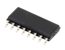
Analog Devices Inc.The AD8275 is a G=0.2 difference amplifier that can be used totranslate +/-10V signals to a +4V level. It solves the problemtypically encountered in industrial and instrumentation where+/-10V signals must be interfaced to a single supply 4V or 5VADC. The AD8275 interfaces the two signal levels, simplifyingdesign.The AD8275 has fast settling time of 450 ns and low distortion,making it suitable for driving medium speed successive approximation(SAR) ADCs. Its wide input voltage range and rail-torailoutputs make it an easy to use building block. Single-supplyoperation reduces the power consumption of the amplifier andhelps to protect the ADC from overdrive conditions. Internal, matched, precision laser-trimmed resistors ensurelow gain error, low gain drift of 1 ppm/°C (maximum), andhigh common-mode rejection of 80 dB. Low offset and lowoffset drift, combined with its fast settling time, make theAD8275 suitable for a variety of data acquisition applicationswhere accurate and quick capture is required. The AD8275 can be used as an analog front end, or it can followbuffers to level translate high voltages to a voltage range acceptedby the ADC. In addition, the AD8275 can be configured fordifferential outputs if used with a differential ADC. The AD8275 is available in a space-saving, 8-lead MSOP and is specified for performance over the −40°C to +85°C temperature range.ApplicationsLevel TranslatorADC DriverInstrumentation Amplifier Building BlockAutomated test equipment
AD9517-0A/PCBZ
Part Number : AD9517-0A/PCBZ
Analog Devices Inc.The AD9517-01 provides a multi-output clock distribution function with subpicosecond jitter performance, along with an on-chip PLL and VCO. The on-chip VCO tunes from 2.55 GHz to 2.95 GHz. Optionally, an external VCO/VCXO of up to 2.4 GHz can be used.The AD9517-0 emphasizes low jitter and phase noise to maximize data converter performance, and it can benefit other applications with demanding phase noise and jitter requirements.The AD9517-0 features four LVPECL outputs (in two pairs) and four LVDS outputs (in two pairs). Each LVDS output can be reconfigured as two CMOS outputs. The LVPECL outputs operate to 1.6 GHz, the LVDS outputs operate to 800 MHz, and the CMOS outputs operate to 250 MHz.For applications that require additional outputs, a crystal reference input, zero-delay, or EEPROM for automatic configuration at startup, the AD9520 and AD9522 are available. In addition, the AD9516 and AD9518 are similar to the AD9517 but have a different combination of outputs.Each pair of outputs has dividers that allow both the divide ratio and coarse delay (or phase) to be set. The range of division for the LVPECL outputs is 1 to 32. The LVDS/CMOS outputs allow a range of divisions up to a maximum of 1024.The AD9517-0 is available in a 48-lead LFCSP and can be operated from a single 3.3 V supply. An external VCO, which requires an extended voltage range, can be accommodated by connecting the charge pump supply (VCP) to 5 V. A separate LVPECL power supply can be from 2.5 V to 3.3 V (nominal).The AD9517-0 is specified for operation over the industrial range of −40°C to +85°C.Applications Low jitter, low phase noise clock distribution 10/40/100 Gb/sec networking line cards, including SONET, Synchronous Ethernet, OTU2/3/4 Forward error correction (G.710) Clocking high speed ADCs, DACs, DDSs, DDCs, DUCs, MxFEs High performance wireless transceivers ATE and high performance instrumentation 1AD9517 is used throughout to refer to all the members of the AD9517 family. However, when AD9517-0 is used, it is refers to that specific member of the AD9517 family.
AD9517-1ABCPZ
Part Number : AD9517-1ABCPZ
Analog Devices Inc.The AD9517-11 provides a multi-output clock distribution function with subpicosecond jitter performance, along with an on-chip PLL and VCO. The on-chip VCO tunes from 2.30 GHz to 2.65 GHz. Optionally, an external VCO/VCXO of up to 2.4 GHz can be used.The AD9517-1 emphasizes low jitter and phase noise to maximize data converter performance, and it can benefit other applications with demanding phase noise and jitter requirements.The AD9517-1 features four LVPECL outputs (in two pairs) and four LVDS outputs (in two pairs). Each LVDS output can be reconfigured as two CMOS outputs. The LVPECL outputs operate to 1.6 GHz, the LVDS outputs operate to 800 MHz, and the CMOS outputs operate to 250 MHz.For applications that require additional outputs, a crystal reference input, zero-delay, or EEPROM for automatic configuration at startup, the AD9520 and AD9522 are available. In addition, the AD9516 and AD9518 are similar to the AD9517 but have a different combination of outputs.Each pair of outputs has dividers that allow both the divide ratio and coarse delay (or phase) to be set. The range of division for the LVPECL outputs is 1 to 32. The LVDS/CMOS outputs allow a range of divisions up to a maximum of 1024.The AD9517-1 is available in a 48-lead LFCSP and can be operated from a single 3.3 V supply. An external VCO, which requires an extended voltage range, can be accommodated by connecting the charge pump supply (VCP) to 5 V. A separate LVPECL power supply can be from 2.5 V to 3.3 V (nominal).The AD9517-1 is specified for operation over the industrial range of −40°C to +85°C.Applications Low jitter, low phase noise clock distribution 10/40/100 Gb/sec networking line cards, including SONET, Synchronous Ethernet, OTU2/3/4 Forward error correction (G.710) Clocking high speed ADCs, DACs, DDSs, DDCs, DUCs, MxFEs High performance wireless transceivers ATE and high performance instrumentation 1AD9517 is used throughout the data sheet to refer to all the members of the AD9517 family. However, when AD9517-1 is used, it is refers to that specific member of the AD9517 family.
AD9520-5/PCBZ
Part Number : AD9520-5/PCBZ
Analog Devices Inc.The AD9520-5 provides a multioutput clock distributionfunction with subpicosecond jitter performance, along withan on-chip PLL that can be used with an external VCO.The AD9520-5 serial interface supports both SPI and I2C ports.An in-package EEPROM, which can be programmed through theserial interface, can store user-defined register settings forpower-up and chip reset.The AD9520-5 features 12 LVPECL outputs in four groups. Anyof the 1.6 GHz LVPECL outputs can be reconfigured as two250 MHz CMOS outputs. If an application requires LVDSdrivers instead of LVPECL drivers, refer to the AD9522-5.Each group of three outputs has a divider that allows both thedivide ratio (from 1 to 32) and the phase offset or coarse timedelay to be set.The AD9520-5 is available in a 64-lead LFCSP and can be operatedfrom a single 3.3 V supply. The external VCO can have anoperating voltage of up to 5.5 V. A separate output driver powersupply can be from 2.375 V to 3.465 V.The AD9520-5 is specified for operation over the standardindustrial range of −40°C to +85°C. Applications Low jitter, low phase noise clock distribution Clock generation and translation for SONET, 10Ge, 10GFC, Synchronous Ethernet, OTU2/3/4 Forward error correction (G.710) Clocking high speed ADCs, DACs, DDSs, DDCs, DUCs, MxFEs High performance wireless transceivers ATE and high performance instrumentation Broadband infrastructures
AD9552BCPZ
Part Number : AD9552BCPZ
Analog Devices Inc.The AD9552 is a fractional-N phase locked loop (PLL) based clock generator designed specifically to replace high frequency crystal oscillators and resonators. The device employs a sigma-delta (Σ-Δ) modulator (SDM) to accommodate fractional frequency synthesis. The user supplies an input reference signal by connecting a single-ended clock signal directly to the REF pin or by connecting a crystal resonator across the XTAL pins.The AD9552 is pin programmable, providing one of 64 standard output frequencies based on one of eight common input frequencies. The device also has a 3-wire SPI interface, enabling the user to program custom input-to-output frequency ratios.The AD9552 relies on an external capacitor to complete the loop filter of the PLL. The output is compatible with LVPECL, LVDS, or single-ended CMOS logic levels, although the AD9552 is implemented in a strictly CMOS process.The AD9552 is specified to operate over the extended industrial temperature range of −40°C to +85°C.APPLICATIONS Cost effective replacement of high frequency VCXO, OCXO, and SAW resonators Extremely flexible frequency translation with low jitter for SONET/SDH (including FEC) , 10 Gb Ethernet, Fibre Channel, and DRFI/DOCSIS High-definition video frequency translation Wireless infrastructure Test and measurement (including handheld devices)
AD9706BCPZ
Part Number : AD9706BCPZ
Analog Devices Inc.The AD9704/AD9705/AD9706/AD9707 are the fourth-generation family in the TxDAC series of high performance, CMOS digital-to-analog converters (DACs). This pin-compatible, 8-/10-/12-/14-bit resolution family is optimized for low power operation, while maintaining excellent dynamic performance. The AD9704/AD9705/AD9706/AD9707 family is pin-compatible with the AD9748/AD9740/AD9742/AD9744 family of TxDAC converters and is specifically optimized for the transmit signal path of communication systems. All of the devices share the same interface, LFCSP package, and pinout, providing an upward or downward component selection path based on performance, resolution, and cost. The AD9704/AD9705/AD9706/AD9707 offers exceptional ac and dc performance, while supporting update rates up to 175 MSPS.The flexible power supply operating range of 1.7 V to 3.6 V and low power dissipation of the AD9704/AD9705/AD9706/AD9707 parts make them well suited for portable and low power applications.Power dissipation of the AD9704/AD9705/AD9706/AD9707 can be reduced to 15 mW, with a small trade-off in performance, by lowering the full-scale current output. In addition, a power-down mode reduces the standby power dissipation to approximately 2.2 mW.The AD9704/AD9705/AD9706/AD9707 has an optional serial peripheral interface (SPI®) that provides a higher level of programmability to enhance performance of the DAC. An adjustable output, common-mode feature allows for easy interfacing to other components that require common modes from 0 V to 1.2 V.Edge-triggered input latches and a 1.0 V temperature-compensated band gap reference have been integrated to provide a complete, monolithic DAC solution. The digital inputs support 1.8 V and 3.3 V CMOS logic families.PRODUCT HIGHLIGHTS Pin Compatible. The AD9704/AD9705/AD9706/AD9707 line of TxDAC converters is pin-compatible with theAD9748/AD9740/AD9742/AD9744 TxDAC line (LFCSP package). Low Power. Complete CMOS DAC operates on a single supply of 3.6 V down to 1.7 V, consuming 50 mW (3.3 V) and 12 mW (1.8 V). The DAC full-scale current can be reduced for lower power operation. Sleep and power-down modes are provided for low power idle periods. Self-Calibration. Self-calibration enables true 14-bit INL and DNL performance in the AD9707. Twos Complement/Binary Data Coding Support. Data input supports twos complement or straight binary data coding. Flexible Clock Input. A selectable high speed, single-ended,and differential CMOS clock input supports 175 MSPS conversion rate. Device Configuration. Device can be configured through pin strapping, and SPI control offers a higher level of programmability. Easy Interfacing to Other Components. Adjustable common-mode output allows for easy interfacing to other signal chain components that accept common-mode levels from 0 V to 1.2 V. On-Chip Voltage Reference. The AD9704/AD9705/AD9706/AD9707 include a 1.0 V temperature-compensated band gap voltage reference. Industry-Standard 32-Lead LFCSP Package.
AD9707-DPG2-EBZ
Part Number : AD9707-DPG2-EBZ
Analog Devices Inc.The AD9704/AD9705/AD9706/AD9707 are the fourth-generation family in the TxDAC series of high performance, CMOS digital-to-analog converters (DACs). This pin-compatible, 8-/10-/12-/14-bit resolution family is optimized for low power operation, while maintaining excellent dynamic performance. The AD9704/AD9705/AD9706/AD9707 family is pin-compatible with the AD9748/AD9740/AD9742/AD9744 family of TxDAC converters and is specifically optimized for the transmit signal path of communication systems. All of the devices share the same interface, LFCSP package, and pinout, providing an upward or downward component selection path based on performance, resolution, and cost. The AD9704/AD9705/AD9706/AD9707 offers exceptional ac and dc performance, while supporting update rates up to 175 MSPS.The flexible power supply operating range of 1.7 V to 3.6 V and low power dissipation of the AD9704/AD9705/AD9706/AD9707 parts make them well suited for portable and low power applications.Power dissipation of the AD9704/AD9705/AD9706/AD9707 can be reduced to 15 mW, with a small trade-off in performance, by lowering the full-scale current output. In addition, a power-down mode reduces the standby power dissipation to approximately 2.2 mW.The AD9704/AD9705/AD9706/AD9707 has an optional serial peripheral interface (SPI®) that provides a higher level of programmability to enhance performance of the DAC. An adjustable output, common-mode feature allows for easy interfacing to other components that require common modes from 0 V to 1.2 V.Edge-triggered input latches and a 1.0 V temperature-compensated band gap reference have been integrated to provide a complete, monolithic DAC solution. The digital inputs support 1.8 V and 3.3 V CMOS logic families.PRODUCT HIGHLIGHTS Pin Compatible. The AD9704/AD9705/AD9706/AD9707 line of TxDAC converters is pin-compatible with theAD9748/AD9740/AD9742/AD9744 TxDAC line (LFCSP package). Low Power. Complete CMOS DAC operates on a single supply of 3.6 V down to 1.7 V, consuming 50 mW (3.3 V) and 12 mW (1.8 V). The DAC full-scale current can be reduced for lower power operation. Sleep and power-down modes are provided for low power idle periods. Self-Calibration. Self-calibration enables true 14-bit INL and DNL performance in the AD9707. Twos Complement/Binary Data Coding Support. Data input supports twos complement or straight binary data coding. Flexible Clock Input. A selectable high speed, single-ended,and differential CMOS clock input supports 175 MSPS conversion rate. Device Configuration. Device can be configured through pin strapping, and SPI control offers a higher level of programmability. Easy Interfacing to Other Components. Adjustable common-mode output allows for easy interfacing to other signal chain components that accept common-mode levels from 0 V to 1.2 V. On-Chip Voltage Reference. The AD9704/AD9705/AD9706/AD9707 include a 1.0 V temperature-compensated band gap voltage reference. Industry-Standard 32-Lead LFCSP Package.
AD9707BCPZRL7
Part Number : AD9707BCPZRL7
Analog Devices Inc.The AD9704/AD9705/AD9706/AD9707 are the fourth-generation family in the TxDAC series of high performance, CMOS digital-to-analog converters (DACs). This pin-compatible, 8-/10-/12-/14-bit resolution family is optimized for low power operation, while maintaining excellent dynamic performance. The AD9704/AD9705/AD9706/AD9707 family is pin-compatible with the AD9748/AD9740/AD9742/AD9744 family of TxDAC converters and is specifically optimized for the transmit signal path of communication systems. All of the devices share the same interface, LFCSP package, and pinout, providing an upward or downward component selection path based on performance, resolution, and cost. The AD9704/AD9705/AD9706/AD9707 offers exceptional ac and dc performance, while supporting update rates up to 175 MSPS.The flexible power supply operating range of 1.7 V to 3.6 V and low power dissipation of the AD9704/AD9705/AD9706/AD9707 parts make them well suited for portable and low power applications.Power dissipation of the AD9704/AD9705/AD9706/AD9707 can be reduced to 15 mW, with a small trade-off in performance, by lowering the full-scale current output. In addition, a power-down mode reduces the standby power dissipation to approximately 2.2 mW.The AD9704/AD9705/AD9706/AD9707 has an optional serial peripheral interface (SPI®) that provides a higher level of programmability to enhance performance of the DAC. An adjustable output, common-mode feature allows for easy interfacing to other components that require common modes from 0 V to 1.2 V.Edge-triggered input latches and a 1.0 V temperature-compensated band gap reference have been integrated to provide a complete, monolithic DAC solution. The digital inputs support 1.8 V and 3.3 V CMOS logic families.PRODUCT HIGHLIGHTS Pin Compatible. The AD9704/AD9705/AD9706/AD9707 line of TxDAC converters is pin-compatible with theAD9748/AD9740/AD9742/AD9744 TxDAC line (LFCSP package). Low Power. Complete CMOS DAC operates on a single supply of 3.6 V down to 1.7 V, consuming 50 mW (3.3 V) and 12 mW (1.8 V). The DAC full-scale current can be reduced for lower power operation. Sleep and power-down modes are provided for low power idle periods. Self-Calibration. Self-calibration enables true 14-bit INL and DNL performance in the AD9707. Twos Complement/Binary Data Coding Support. Data input supports twos complement or straight binary data coding. Flexible Clock Input. A selectable high speed, single-ended,and differential CMOS clock input supports 175 MSPS conversion rate. Device Configuration. Device can be configured through pin strapping, and SPI control offers a higher level of programmability. Easy Interfacing to Other Components. Adjustable common-mode output allows for easy interfacing to other signal chain components that accept common-mode levels from 0 V to 1.2 V. On-Chip Voltage Reference. The AD9704/AD9705/AD9706/AD9707 include a 1.0 V temperature-compensated band gap voltage reference. Industry-Standard 32-Lead LFCSP Package.
AD9717BCPZ
Part Number : AD9717BCPZ
Analog Devices Inc.The AD9714 / AD9715 / AD9716 / AD9717 are pin-compatible, dual, 8-/10-/12-/14-bit, low power digital-to-analog converters (DACs) that provide a sample rate of 125 MSPS. These TxDAC® converters are optimized for the transmit signal path of communication systems. All the devices share the same interface, package, and pinout, providing an upward or downward component selection path based on performance, resolution, and cost.The AD9714 / AD9715 / AD9716 / AD9717 offer exceptional ac and dc performance and support update rates up to 125 MSPS.The flexible power supply operating range of 1.8 V to 3.3 V and low power dissipation of the AD9714 / AD9715 / AD9716 / AD9717 make them well-suited for portable and low power applications.PRODUCT HIGHLIGHTS Low Power. DACs operate on a single 1.8 V to 3.3 V supply; total power consumption reduces to 35 mW at 125 MSPS with a 1.8 V supply. Sleep and power-down modes are provided for low power idle periods. LVCMOS Clock Input. High speed, single-ended LVCMOS clock input supports a 125 MSPS conversion rate. Easy Interfacing to Other Components. Adjustable output common mode from 0 V to 1.2 V allows easy interfacing to other components that accept common- mode levels greater than 0 V.APPLICATIONS Wireless infrastructures Picocell, femtocell base stations Medical instrumentation Ultrasound transducer excitation Portable instrumentation Signal generators, arbitrary waveform generators
ADAU1445YSVZ-3A
Part Number : ADAU1445YSVZ-3A
Analog Devices Inc.The ADAU1442 / ADAU1445 / ADAU1446 are enhanced audio processors that allow full flexibility in routing all input and output signals. The SigmaDSP® core features full 28-bit processing (56-bit in double-precision mode), synchronous parameter loading for ensuring filter stability, and 100% code efficiency with the SigmaStudio™ tools. This DSP allows system designers to compensate for the real-world limitations of speakers, amplifiers, and listening environments, resulting in a dramatic improvement of the perceived audio quality through speaker equalization, multiband compression, limiting, and third-party branded algorithms.The flexible audio routing matrix (FARM) allows the user to multiplex inputs from multiple sources running at various sample rates to or from the SigmaDSP core. This drastically reduces the complexity of signal routing and clocking issues in the audio system. FARM includes up to eight stereo asynchronous sample rate converters (depending on the device model), Sony/Philips Digital Interconnect Format (S/PDIF) input and output, and serial (I2S) and time division multiplexing (TDM) I/Os. Any of these inputs can be routed to the SigmaDSP core or to any of the asynchronous sample rate converters (ASRCs). Similarly, any one of the output signals can be taken from the SigmaDSP core or from any of the ASRC outputs. This routing scheme, which can be modified at any time via control registers, allows for maximum system flexibility.The ADAU1442, ADAU1445, and ADAU1446 differ only in ASRC functionality and packaging. The ADAU1442/ADAU1445 contain 16 channels of ASRCs and are packaged in TQFP packages, whereas the ADAU1446 contains no ASRCs and is packaged in an LQFP. The ADAU1442 can handle nine clock domains, the ADAU1445 can handle three clock domains, and the ADAU1446 can handle one clock domain.The ADAU1442 / ADAU1445 / ADAU1446 can be controlled in one of two operational modes: the settings of the chip can be loaded and dynamically updated through the SPI/I2C® port, or the DSP can self-boot from an external EEPROM in a system with no microcontroller. There is also a bank of multipurpose (MP) pins that can be used as general-purpose digital I/Os or as inputs to the 4-channel auxiliary control ADC.The ADAU1442 / ADAU1445 / ADAU1446 are supported by the SigmaStudio graphical development environment. This software includes audio processing blocks such as FIR and IIR filters, dynamics processors, mixers, low level DSP functions, and third-party algorithms for fast development of custom signal flows.APPLICATIONS Automotive audio processing Head units Navigation systems Rear-seat entertainment systems DSP amplifiers (sound system amplifiers) Commercial audio processing
ADM1491EBRMZ
Part Number : ADM1491EBRMZ
Analog Devices Inc.The ADM1490E / ADM1491E are RS-485 transceivers with ±8 kV ESD protection and is suitable for high speed, full-duplex communication on multipoint transmission lines. In particular, the ADM1491E is designed for use in motor control applications requiring communications at data rates up to 16 Mbps.The ADM1491E is designed for balanced transmission lines and complies with TIA/EIA-485-A-98. The device has a 12 kΩ receiver input impedance for unit load RS-485 operation allowing up to 32 nodes on the bus.The differential transmitter outputs and receiver inputs feature electrostatic discharge circuitry that provides protection to ±8 kV using the human body model (HBM).The ADM1491E operates from a single 5 V power supply. Excessive power dissipation caused by bus contention or output shorting is prevented by short-circuit protection and thermal circuitry.Short-circuit protection circuits limit the maximum output current to ±250 mA during fault conditions. A thermal shutdown circuit senses if the die temperature rises above 150°C and forces the driver outputs into a high impedance state under this condition.The receiver of the ADM1491E contains a fail-safe feature that results in a logic high output state if the inputs are unconnected (floating).The ADM1491E features extremely fast and closely matched switching times. Minimal driver propagation delays permit transmission at data rates up to 16 Mbps while low skew minimizes EMI interference.The ADM1491E is fully specified over the commercial and industrial temperature ranges and is available in two packages: a narrow-body 14-lead SOIC and a 10-lead MSOP.APPLICATIONS RS-485/RS-422 interfaces Industrial field networks High data rate motor control Multipoint data transmission systems Single-ended to differential signal conversion
ADM2484EBRWZ-REEL7
Part Number : ADM2484EBRWZ-REEL7
Analog Devices Inc.The ADM2484E is an isolated data transceiver with ±15 kVESD protection suitable for high speed, half- or full-duplex communication on multipoint transmission lines. For half-duplex operation, the transmitter outputs and receiver inputs share the same transmission line. Transmitter Output Pin Y links externally to Receiver Input Pin A, and Transmitter Output Pin Z links externally to Receiver Input Pin B.Designed for balanced transmission lines, the ADM2484Ecomplies with ANSI TIA/EIA RS-485-A-1998 and ISO 8482: 1987(E). The device employs Analog Devices, Inc., iCoupler® technology to combine a 3-channel isolator, a three-state differential line driver, and a differential input receiver into a single package.The differential transmitter outputs and receiver inputs featureelectrostatic discharge circuitry that provides protection up to ±15 kV using the human body model (HBM). The logic side of the device can be powered with either a 5 V or a 3.3 V supply, whereas the bus side requires an isolated 3.3 V supply.The device has current-limiting and thermal shutdown featuresto protect against output short circuits and situations where buscontention causes excessive power dissipation.Applications Isolated RS-485/RS-422 interfaces Industrial field networks INTERBUS Multipoint data transmission systems
ADN4661BRZ
Part Number : ADN4661BRZ
Analog Devices Inc.The ADN4661 is a single, CMOS, low voltage differential signaling (LVDS) line driver offering data rates of over 600 Mbps (300 MHz) and ultra-low power consumption. It features a flow-through pinout for easy PCB layout and separation of input and output signals.The device accepts low voltage TTL/CMOS logic signals and converts them to a differential current output of typically ±3.1 mA for driving a transmission medium such as a twisted-pair cable. The transmitted signal develops a differential voltage of typically ±355 mV across a termination resistor at the receiv-ing end, and this is converted back to a TTL/CMOS logic level by a line receiver.The ADN4661 and a companion LVDS receiver offer a new solution to high speed point-to-point data transmission, and a low power alternative to emitter-coupled logic (ECL) or positive emitter-coupled logic (PECL).ApplicationsBackplane data transmissionCable data transmissionClock distribution
ADN4668ARZ
Part Number : ADN4668ARZ
Analog Devices Inc.The ADN4668 is a quad-channel CMOS, low voltage differential signaling (LVDS) line receiver offering data rates of over 400 Mbps (200 MHz) and ultralow power consumption. It features a flow-through pin configuration for easy PCB layout and separation of input and output signals. The device accepts low voltage (310 mV typical) differential input signals and converts them to a single-ended, 3 V TTL/CMOS logic level.The ADN4668 also offers active-high and active-low enable/disable inputs (EN and overbar: EN) that control all four receivers. They disable the receivers and switch the outputs to a high impedance state. This high impedance state allows the outputs of one or more ADN4668s to be multiplexed together and reduces the quies-cent power consumption to 3 mW typical. The ADN4668 and its companion driver, the ADN4667, offer a new solution to high speed, point-to-point data transmission and a low power alternative to emitter-coupled logic (ECL) or positive emitter-coupled logic (PECL).
ADP1753ACPZ-R7
Part Number : ADP1753ACPZ-R7
Analog Devices Inc.The ADP1752 / ADP1753 are CMOS, low dropout linear regulators that operate from 1.6 V to 3.6 V and provide up to 800mA of output current. These low VIN & VOUT LDOs are ideal for regulation of nanometer FPGA geometries operating from 2.5V down to 1.8V I/O rails, and powering core voltages down to 0.75V. Using an advanced proprietary architecture, they provide high power supply rejection, low noise, and achieve excellent line and load transient response with a small 4.7 µF ceramic output capacitor.The ADP1752 is available in 7 fixed output voltage options. The ADP1753 is available in an adjustable version, which allows output voltages that range from 0.75 V to 3.0 V via an external divider. The ADP1752 / ADP1753 allows an external soft start capacitor to be connected to program the start-up. A power good output allows power system monitors to digitally check the health of the output power rail voltage.The ADP1752 / ADP1753 are available in a 16-lead, 4 mm × 4 mm LFCSP, making them not only very compact solutions, but also providing excellent thermal performance for applications requiring up to 800mA of output current in a small, low profile footprint.APPLICATIONS Server computers Memory components Telecommunications equipment Network equipment DSP/FPGA/microprocessor supplies Instrumentation equipment/data acquisition systems
ADR423ARMZ
Part Number : ADR423ARMZ
Analog Devices Inc. he ADR42x are a series of ultraprecision, second generation eXtra implanted junction FET (XFET) voltage references featuring low noise, high accuracy, and excellent long-term stability in SOIC and MSOP footprints.Patented temperature drift curvature correction technique and XFET technology minimize nonlinearity of the voltage change with temperature. The XFET architecture offers superior accuracy and thermal hysteresis to the band gap references. It also operates at lower power and lower supply headroom than the buried Zener references.The superb noise and the stable and accurate characteristics of the ADR42x make them ideal for precision conversion applications such as optical networks and medical equipment. The ADR42x trim terminal can also be used to adjust the out-put voltage over a ±0.5% range without compromising any other performance. The ADR42x series voltage references offer two electrical grades and are specified over the extended industrial temperature range of −40°C to +125°C. Devices have 8-lead SOIC or 30% smaller, 8-lead MSOP packages.APPLICATIONS Precision data acquisition systems High resolution converters Battery-powered instrumentation Portable medical instruments Industrial process control systems Precision instruments Optical network control circuits
ADR445BRZ-REEL7
Part Number : ADR445BRZ-REEL7
Analog Devices Inc.The ADR440/ADR441/ADR443/ADR444/ADR445 series is a family of XFET® voltage references featuring ultralow noise, high accuracy, and low temperature drift performance. Using Analog Devices, Inc., patented temperature drift curvature correction and XFET (eXtra implanted junction FET) technology, voltage change vs. temperature nonlinearity in the ADR440/ADR441/ADR443/ADR444/ADR445 is greatly minimized.The XFET references offer better noise performance than buried Zener references, and XFET references operate off low supply voltage headroom (500 mV). This combination of features makes the ADR440/ADR441/ADR443/ADR444/ADR445 family ideally suited for precision signal conversion applications in high-end data acquisition systems, optical networks, and medical applications.The ADR440/ADR441/ADR443/ADR444/ADR445 family has the capability to source up to 10 mA of output current and sink up to −5 mA. It also comes with a trim terminal to adjust the output voltage over a 0.5% range without compromising performance.The ADR440/ADR441/ADR443/ADR444/ADR445 family is available in 8-lead MSOP and narrow SOIC packages and offered in two electrical grades. All versions are specified over the extended industrial temperature range of −40°C to +125°C.Applications Precision data acquisition systems High resolution data converters Battery-powered instrumentation Portable medical instruments Industrial process control systems Precision instruments Optical control circuits
ADSP-BF512BBCZ-4
Part Number : ADSP-BF512BBCZ-4
Analog Devices Inc.The ADSP-BF512 is the low cost entry point into the Blackfin Processor family. It offers an optimal balance between performance, peripheral integration, and price and is well suited for the most cost-sensitive applications including portable test equipment, embedded modems, biometrics, and consumer audio. The high performance 16/32-bit Blackfin embedded processor core, the flexible cache architecture, the enhanced DMA subsystem, and the dynamic power management (DPM) functionality allow system designers a flexible platform to address a wide range of applications.IP protection has become a necessary part of today’s embedded computing applications. The ADSP-BF512 provides a security scheme which balances flexibility and upgradeability with performance through the inclusion of a firmware-based solution including OTP (One Time Programmable) memory to enable users to implement private keys for secure access to program code.
ADSP-BF512KSWZ-4
Part Number : ADSP-BF512KSWZ-4
Analog Devices Inc.The ADSP-BF512 is the low cost entry point into the Blackfin Processor family. It offers an optimal balance between performance, peripheral integration, and price and is well suited for the most cost-sensitive applications including portable test equipment, embedded modems, biometrics, and consumer audio. The high performance 16/32-bit Blackfin embedded processor core, the flexible cache architecture, the enhanced DMA subsystem, and the dynamic power management (DPM) functionality allow system designers a flexible platform to address a wide range of applications.IP protection has become a necessary part of today’s embedded computing applications. The ADSP-BF512 provides a security scheme which balances flexibility and upgradeability with performance through the inclusion of a firmware-based solution including OTP (One Time Programmable) memory to enable users to implement private keys for secure access to program code.
ADSP-BF514KSWZ-3
Part Number : ADSP-BF514KSWZ-3
Analog Devices Inc.The ADSP-BF512 / ADSP-BF514 / ADSP-BF516 / ADSP-BF518 processors are members of the Blackfin® family of products, incorporating the Analog Devices/Intel Micro Signal Architecture (MSA). Blackfin processors combine a dual-MAC state-of-the-art signal processing engine, the advantages of a clean, orthogonal RISC-like microprocessor instruction set, and single-instruction, multiple-data (SIMD) multimedia capabilities into a single instruction-set architecture.The processors are completely code compatible with other Blackfin processors.MEMORY 116K bytes of on-chip memory External memory controller with glueless support for SDRAM and asynchronous 8-bit and 16-bit memories Flexible booting options from OTP memory, external SPI/parallel memories, or from SPI/UART host devices Code security with Lockbox secure technology One-time-programmable (OTP) memory Memory management unit providing memory protectionSee datasheet for additional features


