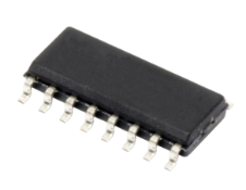
AD5306BRUZ
Part Number : AD5306BRUZ
Analog Devices Inc.The AD5306 / AD5316 / AD5326 are quad 8-, 10-, and 12-bit buffered voltage output DACs, in a 16-lead TSSOP package, that operate from a single 2.5 V to 5.5 V supply, consuming 500 µA at 3 V. Their on-chip output amplifiers allow rail-to-rail output swing with a slew rate of 0.7 V/μs. A 2-wire serial interface that operates at clock rates up to 400 kHz is used. This interface is SMBus-compatible at VDD
AD539JNZ
Part Number : AD539JNZ
Analog Devices Inc.The AD539 is a low distortion analog multiplier having two identical signal channels (Y1 and Y2), with a common X input providing linear control of gain. Excellent ac characteristics up to video frequencies and a −3 dB bandwidth of over 60 MHz are provided. Although intended primarily for applications where speed is important, the circuit exhibits good static accuracy in computational applications. Scaling is accurately determined by a band-gap voltage reference and all critical parameters are laser-trimmed during manufacture.The full bandwidth can be realized over most of the gain range using the AD539 with simple resistive loads of up to 100 Ω. Output voltage is restricted to a few hundred millivolts under these conditions. The two channels provide flexibility. In single-channel applications, they can be used in parallel to double the output current, in series to achieve a square-law gain function with a control range of over 100 dB, or differentially to reduce distortion. Alternatively, they can be used independently, as in audio stereo applications, with low crosstalk between channels. Voltage-controlled filters and oscillators using the state-variable approach are easily designed, taking advantage of the dual channels and common control. The AD539 can also be configured as a divider with signal bandwidths up to 15 MHz.Power consumption is only 135 mW using the recommended ±5 V supplies. The AD539 is available in three versions: the J and K grades are specified for 0 to 70°C operation and S grade is guaranteed over the extended range of −55°C to +125°C. The J and K grades are available in either a hermetic ceramic SBDIP (D-16) or a low cost PDIP (N-16), whereas the S grade is available in ceramic SBDIP (D-16) or LCC (E-20-1). The S grade is available in MIL-STD-883 and Standard Military Drawing (DESC) Number 5962-8980901EA versions.APPLICATIONS Precise high bandwidth AGC and VCA systems Voltage-controlled filters Video signal processing High speed analog division Automatic signal-leveling Square-law gain/loss control
AD5432YRMZ
Part Number : AD5432YRMZ
Analog Devices Inc.The AD5426 / AD5432 / AD5443 are CMOS 8-, 10-, and 12-bit current output digital-to-analog converters (DACs), respectively. These devices operate from a 2.5 V to 5.5 V power supply, making them suitable for battery-powered applications and many other applications.These DACs use a double buffered, 3-wire serial interface that is compatible with SPI, QSPI™, MICROWIRE™, and most DSP interface standards. In addition, a serial data out pin (SDO) allows for daisy-chaining when multiple packages are used. Data readback allows the user to read the contents of the DAC register via the SDO pin. On power-up, the internal shift register and latches are filled with 0s and the DAC outputs are at zero scale.As a result of manufacturing on a CMOS submicron process, the parts offer excellent 4-quadrant multiplication characteristics with large signal multiplying bandwidths of 10 MHz. The applied external reference input voltage, VREF, determines the full-scale output current. An integrated feedback resistor, RFB, provides temperature tracking and full-scale voltage output when combined with an external current to voltage precision amplifier.The AD5426 / AD5432 / AD5443 DACs are available in small, 10-lead MSOP packages.The EVAL-AD5443SDZ / EVAL-AD5446SDZ / EVAL-AD5453SDZ evaluation board is available for evaluating DAC performance. For more information, see the UG-327 evaluation board user guide.APPLICATIONS Portable battery-powered applications Waveform generators Instrumentation Programmable amplifiers and attenuators Digitally controlled calibration Programmable filters and oscillators Composite video Ultrasound Gain, offset, and voltage trimming
AD580KH
Part Number : AD580KH
Analog Devices Inc.The AD580 is a three-terminal, low cost, temperature compensated, bandgap voltage reference which provides a fixed 2.5 V output for inputs between 4.5 V and 30 V. A unique combination of advanced circuit design and laser-wafer trimmed thin-film resistors provide the AD580 with an initial tolerance of ±0.4%, a temperature stability of better than 10 ppm/°C and long-term stability of better than 250µV. In addition, the low quiescent current drain of 1.5 mA max offers a clear advantage over classical Zener techniques.The AD580 is recommended as a stable reference for all 8-, 10- and 12-bit D-to-A converters that require an external reference. In addition, the wide input range of the AD580 allows operation with 5 volt logic supplies making the AD580 ideal for digital panel meter applications or whenever only a single logic power supply is available. The AD580J, K, L and M are specified for operation over the 0°C to +70°C temperature range; the AD580S, T and U are specified for operation over the extended temperature range of -55°C to +125°C.
AD581LH
Part Number : AD581LH
Analog Devices Inc.The AD581 is a 3-pin, temperature compensated, monolithic, band gap voltage reference that provides a precise 10.00 V output from an unregulated input level ranging from 12 V to 30 V. Laser wafer trimming (LWT) is used to trim both the initial error at +25°C as well as the temperature coefficient, resulting in high precision performance previously available only in expensive hybrids or oven regulated modules. The 5 mV initial error tolerance and 5 ppm/°C guaranteed temperature coefficient of the AD581L is available in a monolithic voltage reference.The band gap circuit design used in the AD581 offers several advantages over classical Zener breakdown diode techniques. Most important, no external components are required to achieve full accuracy and significant stability to low power systems. In addition, total supply current to the device, including the output buffer amplifier (which can supply up to 10 mA) is typically 750 μA. The long-term stability of the band gap design is equivalent to selected Zener reference diodes.The AD581 is recommended for use as a reference for 8-, 10- or 12-bit digital-to-analog converters (DACs) that require an external precision reference. The device is also ideal for all types of analog-to-digital converters (ADCs) up to 14-bit accuracy, either successive approximation or integrating designs, and can generally offer better performance than that provided by standard self-contained references.The AD581J, K, and L are specified for operation from 0°C to +70°C; the AD581S, T, and U are specified for the -55°C to +125°C range. All grades are packaged in a hermetically sealed three-terminal TO-5 metal can.PRODUCT HIGHLIGHTS Laser trimming of both initial accuracy and temperature coefficient results in very low errors over temperature without the use of external components. The AD581L has a maximum deviation from 10.000 V of ±7.25 mV from 0°C to 70°C, whereas the AD581U guarantees ±15 mV maximum total error without external trims from −55°C to +125°C. Because the laser trimming is done on the wafer prior to separation into individual chips, the AD581 is extremely valuable to hybrid designers for its ease of use, lack of required external trims, and inherent high performance. The AD581 can also be operated in a 2-pin Zener mode to provide a precision −10 V reference with just one external resistor to the unregulated supply. The performance in this mode is nearly equal to that of the standard 3-pin configuration. Advanced circuit design using the band gap concept allows the AD581 to give full performance with an unregulated input voltage down to 13 V. With an external resistor, the device operates with a supply as low as 11.4 V. 5. The AD581 is available in versions compliant with MILSTD-883. Refer to the military datasheet for detailed specifications.
AD625CDZ
Part Number : AD625CDZ
Analog Devices Inc.The AD625 is a precision instrumentation amplifier specifically designed to fulfill two major areas of application: 1) Circuits requiring nonstandard gains (i.e., gains not easily achievable with devices such as the AD524 and AD624). 2) Circuits requiring a low cost, precision software programmable gain amplifier.For low noise, high CMRR, and low drift the AD625JN is the most cost effective instrumentation amplifier solution available. An additional three resistors allow the user to set any gain from 1 to 10,000. The error contribution of the AD625JN is less than 0.05% gain error and under 5 ppm/°C gain TC; performance limitations are primarily determined by the external resistors. Common-mode rejection is independent of the feedback resistor matching.A software programmable gain amplifier (SPGA) can be configured with the addition of a CMOS multiplexer (or other switch network), and a suitable resistor network. Because the ON resistance of the switches is removed from the signal path, an AD625 based SPGA will deliver 12-bit precision, and can be programmed for any set of gains between 1 and 10,000, with completely user selected gain steps.For the highest precision the AD625C offers an input offset voltage drift of less than 0.25 µV/°C, output offset drift below 15 µV/°C, and a maximum nonlinearity of 0.001% at G = 1. All grades exhibit excellent ac performance; a 25 MHz gain bandwidth product, 5 V/µs slew rate and 15 µs settling time.The AD625 is available in three accuracy grades (A, B, C) for industrial (-40°C to +85°C) temperature range, two grades (J, K) for commercial (0°C to +70°C) temperature range, and one (S) grade rated over the extended (-55°C to +125°C) temperature range.
AD6620ASZ
Part Number : AD6620ASZ
Analog Devices Inc.Analog Devices' innovative Diversity Receiver chipset delivers two IF-to-baseband diversity channels in a compact, comprehensive solutionthat incorporates Automatic Gain Control, Received Signal Strength Indicator, high-resolution. Numerically Controlled Oscillator and digital filtering on-chip.The chipset comprises Analog Devices' AD6600 dual-channel IF sampling analog-to-digital converter and AD6620 dual-channel decimatingreceiver chip. Configured with the appropriate external components, it can address a variety of air interface standards, including GSM, CDMA,IS136 and PHS, as well as proprietary modulation schemes for paging systems and wireless fixed access receivers.Based on Analog Devices' next-generation receiver architecture, the Diversity Receiver replaces sensitive analog filters with digital filters for significant cost and size reductions. Complete reference designs show the optimal layout for reducing noise and minimizing cross-channel coupling.
AD7247AANZ
Part Number : AD7247AANZ
Analog Devices Inc.The AD7237A / AD7247A is an enhanced version of the industry standard AD7237 / AD7247. Improvements include operation from 12 V to 15 V supplies, faster interface times and better reference variations with VDD. Additional features include faster settling times.The AD7237A / AD7247A is a complete, dual, 12-bit, voltage output digital-to-analog converter with output amplifiers and Zener voltage reference on a monolithic CMOS chip. No external user trims are required to achieve full specified performance.Both parts are microprocessor compatible, with high speed data latches and interface logic. The AD7247A accepts 12-bit parallel data which is loaded into the respective DAC latch using the WR input and a separate Chip Select input for each DAC. The AD7237A has a double buffered interface structure and an 8-bit wide data bus with data loaded to the respective input latch in two write operations. An asynchronous LDAC signal on the AD7237A updates the DAC latches and analog outputs.A REF OUT/REF IN function is provided which allows either the on-chip 5 V reference or an external reference to be used as a reference voltage for the part. For single supply operation, two output ranges of 0 V to +5 V and 0 V to +10 V are available, while these two ranges plus an additional ±5 V range are available with dual supplies. The output amplifiers are capable of developing +10 V across a 2 kΩ load to GND.The AD7237A / AD7247A is fabricated in Linear Compatible CMOS (LC2MOS), an advanced, mixed technology process that combines precision bipolar circuits with low power CMOS logic. Both parts are available in a 24-pin, 0.3' wide plastic and hermetic dual-in-line package (DIP) and are also packaged in a 24-lead small outline (SOIC) package.
AD7390ARZ
Part Number : AD7390ARZ
Analog Devices Inc.The AD7390 / AD7391 family of 10- and 12-bit voltage-output digital-to-analog converters are designed to operate from a single +3 volt supply. Built using a CBCMOS process, these monolithic DACs offer the user low cost, and ease-of-use in single-supply +3 V volt systems. Operation is guaranteed over the supply voltage range of +2.7 V to +5.5 V consuming less than 100 µA making this device ideal for battery operated applications.The full-scale voltage output is determined by the external reference input voltage applied. The rail-to-rail REFIN to DACOUT allows for a full-scale voltage set equal the positive supply VDD or any value in between.A doubled-buffered serial-data interface offers high-speed, three-wire, SPI and microcontroller compatible inputs using data in (SDI), clock (CLK) and load strobe (LD) pins. Additionally, a CLR input sets the output to zero scale at power on or upon user demand.Both parts are offered in the same pin out to allow the user to select the amount of resolution appropriate for their application without circuit card redesign.The AD7390 / AD7391 are specified over the extended industrial (-40°C to +85°C) temperature range. The AD7391AR is specified for the -40°C to +125°C automotive temperature range. The AD7390 / AD7391s are available in plastic DIP, and low profile 1.75 mm height SO-8 surface mount packages. The AD7391ARU is available for ultracompact applications in a thin 1.1 mm TSSOP-8 package.APPLICATIONS Automotive 0.5 V to 4.5 V Output Span Voltage Portable Communications Digitally Controlled Calibration
AD7655ASTZ
Part Number : AD7655ASTZ
Analog Devices Inc.The AD7655 is a low cost, simultaneous sampling, dual-channel,16-bit, charge redistribution SAR, analog-to-digital converterthat operates from a single 5 V power supply. It contains twolow noise, wide bandwidth, track-and-hold amplifiers that allowsimultaneous sampling, a high speed 16-bit sampling ADC, aninternal conversion clock, error correction circuits, and bothserial and parallel system interface ports. Each track-and-holdhas a multiplexer in front to provide a 4-channel input ADC.The A0 multiplexer control input allows the choice ofsimultaneously sampling input pairs INA1/INB1 (A0 = low) orINA2/INB2 (A0 = high). The part features a very high samplingrate mode (normal) and, for low power applications, a reducedpower mode (impulse) where the power is scaled with thethroughput. Operation is specified from −40°C to +85°C.Product Highlights Multichannel ADC. The AD7655 features 4-channel inputs with two sample-and-hold circuits that allow simultaneous sampling. Fast Throughput. The AD7655 is a 500 kSPS, charge redistribution, 16-bit SAR ADC with internal error correction circuitry. Single-Supply Operation. The AD7655 operates from a single 5 V supply. In impulse mode, its power dissipation decreases with throughput. Serial or Parallel Interface. Versatile parallel or 2-wire serial interface arrangements are compatible with both 3 V and 5 V logic.Applications AC motor control 3-phase power control 4-channel data acquisition Uninterrupted power supplies Communications
AD7663ACPZ
Part Number : AD7663ACPZ
Analog Devices Inc.Based on the Pulsar core, the AD7663 is a bipolar 16-bit, 250 kSPS, charge redistribution SAR Analog-to-Digital Converter that operates from a single 5 V power supply. It contains a high-speed 16-Bit sampling ADC, a resistor input scalar that allows various input ranges, an internal conversion clock, error correction circuits, and both serial and parallel system interface ports.The AD7663 is hardware factory-calibrated and is comprehensively tested to ensure such ac parameters as signal-to-noise ratio(SNR) and total harmonic distortion (THD), in addition to themore traditional dc parameters of gain, offset, and linearity.It is fabricated using Analog Devices’ high performance, 0.6 micronCMOS process and is available in a 48-lead LQFP and a tiny48-lead LFCSP with operation specified from –40°C to +85°C.PRODUCT HIGHLIGHTS Fast Throughput The AD7663 is a 250 kSPS charge redistribution, 16-bit SAR ADC with various bipolar and unipolar input ranges. Single-Supply Operation The AD7663 operates from a single 5 V supply and dissipates only 35 mW typical. Its power dissipation decreases with the throughput to, for instance, only 15 µW at a 100 SPS throughput. It consumes 7 µW maximum when in power-down. Superior INL The AD7663 has a maximum integral nonlinearity of 3 LSB with no missing 16-bit code. Serial or Parallel Interface Versatile parallel (8 bits or 16 bits) or 2-wire serial interface arrangement compatible with both 3 V or 5 V logic.APPLICATIONS Data Acquisition Motor Control Communication Instrumentation Spectrum Analysis Medical Instruments Process Control
AD7663ASTZ
Part Number : AD7663ASTZ
Analog Devices Inc.Based on the Pulsar core, the AD7663 is a bipolar 16-bit, 250 kSPS, charge redistribution SAR Analog-to-Digital Converter that operates from a single 5 V power supply. It contains a high-speed 16-Bit sampling ADC, a resistor input scalar that allows various input ranges, an internal conversion clock, error correction circuits, and both serial and parallel system interface ports.The AD7663 is hardware factory-calibrated and is comprehensively tested to ensure such ac parameters as signal-to-noise ratio(SNR) and total harmonic distortion (THD), in addition to themore traditional dc parameters of gain, offset, and linearity.It is fabricated using Analog Devices’ high performance, 0.6 micronCMOS process and is available in a 48-lead LQFP and a tiny48-lead LFCSP with operation specified from –40°C to +85°C.PRODUCT HIGHLIGHTS Fast Throughput The AD7663 is a 250 kSPS charge redistribution, 16-bit SAR ADC with various bipolar and unipolar input ranges. Single-Supply Operation The AD7663 operates from a single 5 V supply and dissipates only 35 mW typical. Its power dissipation decreases with the throughput to, for instance, only 15 µW at a 100 SPS throughput. It consumes 7 µW maximum when in power-down. Superior INL The AD7663 has a maximum integral nonlinearity of 3 LSB with no missing 16-bit code. Serial or Parallel Interface Versatile parallel (8 bits or 16 bits) or 2-wire serial interface arrangement compatible with both 3 V or 5 V logic.APPLICATIONS Data Acquisition Motor Control Communication Instrumentation Spectrum Analysis Medical Instruments Process Control
AD7708BRZ
Part Number : AD7708BRZ
Analog Devices Inc.The AD7708 / AD7718 are complete analog front-ends for low frequency measurement applications. The AD7718 contains a 24-bit sigma delta ADC with PGA and can be configured as 4/5 fully-differential input channels or 8/10 pseudo-differential input channels. Two pins on the device are configurable as analog inputs or reference inputs. The AD7708 is a 16-bit version of the AD7718. Inputs signal ranges from 20mV to 2.56V can be directly converted using these ADCs. Signals can be converted directly from a transducer without the need for signal conditioning.The device operates from a 32 kHz crystal with an on-board PLL generating the required internal operating frequency. The output data rate from the part is software programmable. The peak-to-peak resolution from the part varies with the programmed gain and output data ratThe part operates from a single 3 V or 5 V supply. When operating from 3 V supplies, the power dissipation for the part is 3.84 mW typ. Both parts are pin-for-pin compatible allowing an upgradable path from 16 to 24 bits without the need for hardware modifications. The AD7708 / AD7718 are housed in 28-lead SOIC and TSSOP packagesAPPLICATIONS Industrial Process Control Instrumentation Pressure Transducers Portable Instrumentation Smart Transmitters
AD7730BRUZ
Part Number : AD7730BRUZ
Analog Devices Inc.The AD7730 is a complete analog front end for weigh-scale and pressure measurement applications. The device accepts low-level signals directly from a transducer and outputs a serial digital word. The input signal is applied to a proprietary programmable gain front end based around an analog modulator.The modulator output is processed by a low pass programmable digital filter, allowing adjustment of filter cutoff, output rate and settling time.The part features two buffered differential programmable gain analog inputs as well as a differential reference input. The part operates from a single +5 V supply. It accepts four unipolar analog input ranges: 0 mV to ±10 mV, +20 mV, +40 mV and +80 mV and four bipolar ranges: ±10 mV, ±20 mV, ±40 mV and ±80 mV. The peak-to-peak resolution achievable directly from the part is 1 in 230,000 counts. An on-chip 6-bit DAC allows the removal of TARE voltages. Clock signals for synchronizing ac excitation of the bridge are also provided.The serial interface on the part can be configured for three-wire operation and is compatible with microcontrollers and digital signal processors. The AD7730 contains self-calibration and system calibration options, and features an offset drift of less than 5 nV/°C and a gain drift of less than 2 ppm/°C.The part is available in a 24-pin plastic DIP, a 24-lead SOIC and 24-lead TSSOP package.APPLICATIONS Weigh Scales Pressure Measurement
AD7730LBRZ
Part Number : AD7730LBRZ
Analog Devices Inc.The AD7730L is a complete analog front end for weigh-scale and pressure measurement applications. The device accepts low-level signals directly from a transducer and outputs a serial digital word. Theinput signal is applied to a proprietary programmable gain front end based around an analog modulator. The modulator output is processed by a low pass programmable digital filter, allowing adjustment of filter cutoff, output rate and settling time.The part features two buffered differential programmable gain analog inputs as well as a differential reference input. The device operates from a single +5 V supply. It accepts four unipolar analog input ranges: 0 mV to +10 mV, +20 mV, +40 mV and +80 mV and four bipolar ranges: ±10 mV, ±20 mV, ±40 mV and ±80 mV. The peak-to-peak resolution achievable directly from the part is 1 in 110,000 counts. An on-chip 6-bit DAC allows the removal of TARE voltages. Clock signals for synchronizing ac excitation of the bridge are also provided.The serial interface on the part can be configured for three-wire operation and is compatible with microcontrollers and digital signal processors. The AD7730L contains self-calibration and system calibration options, and features an offset drift of less than 5 nV/°C and a gain drift of less than 3 ppm/°C. The part is available in a 24-lead SOIC and 24-lead TSSOP package. It is a lower power version of the AD7730 (approximately 1/3 the power).
AD7788ARMZ
Part Number : AD7788ARMZ
Analog Devices Inc.The AD7788/AD7789 are low power, low noise, analog frontends for low frequency measurement applications. The AD7789contains a low noise, 24-bit, ∑-∆ analog-to-digital converter(ADC) with one differential input. The AD7788 is a 16-bitversion of the AD7789.The devices operate from an internal clock. Therefore, the userdoes not have to supply a clock source to the devices. The outputdata rate is 16.6 Hz, which gives simultaneous 50 Hz/60 Hzrejection.The devices operate with a single power supply from 2.5 V to5.25 V. When operating from a 3 V supply, the power dissipationfor the device is 225 µW maximum. The AD7788/AD7789 areavailable in a 10-lead MSOP.Applications Smart transmitters Battery applications Portable instrumentation Sensor measurement Temperature measurement Pressure measurement Weigh scales 4 to 20 mA loops
AD7871JPZ
Part Number : AD7871JPZ
Analog Devices Inc.The AD7871 / AD7872 are fast, complete, 14-bit analog-to-digital converters (ADC). They consist of a track-and-hold amplifier, successive approximation ADC, 3 V buried Zener reference, and versatile interface logic. The ADC features a self-contained, laser trimmed internal clock, so no external clock timing components are required. The on-chip clock may be overridden to synchronize ADC operation to the digital system for minimum noise.The AD7871 offers a choice of three data output formats: a single, parallel, 14-bit word; two 8-bit bytes or a 14-bit serial data stream. The AD7872 is a serial output device only. The two parts are capable of interfacing to all modern microprocessors and digital signal processors.The AD7871 / AD7872 operate from ±5 V power supplies, accept bipolar input signals of ±3 V and can convert full power signals up to 41.5 kHz.In addition to the traditional dc accuracy specifications, the AD7871 / AD7872 are also fully specified for dynamic performance parameters including distortion and signal-to-noise ratio.Both devices are fabricated in Analog Devices, Inc., LC2MOS mixed technology process. The AD7871 is available in 28-pin PDIP, PLCC, and CERDIP packages. The AD7872 is available in a 16-pin PDIP, CERDIP, and SOIC packages.
ADV7613BBCZ
Part Number : ADV7613BBCZ
Analog Devices Inc.The ADV7613 is a high quality, low power, single-input HDMIto LVDS display bridge. It incorporates an HDMI capablereceiver that supports up to 1080p, 60 Hz.The HDMI port has dedicated 5 V detect and hot plug assert pins. The HDMI receiver also includes an integrated equalizer that ensures the robust operation of the interface with longcables.The ADV7613 has an audio output port for the audio dataextracted from the HDMI stream. HDMI audio formats includesuper audio CD (SACD) via Direct Stream Digital® (DSD) andHBR. The HDMI receiver has an advanced mute controller that prevents audible extraneous noise in the audio output.The ADV7613 contains a component processor (CP) that processes the video signals from the HDMI receiver. It providesfeatures such as contrast, brightness and saturation adjustments, STDI detection block, free run, and synchronization alignment controls.The LVDS encoder can package data into 6-bit or 8-bit non-dcbalanced OpenLDI mapping or 8-bit VESA mapping. TheADV7613 can output 24-bit OpenLDI data via dual-channelLVDS transmitters, up to a maximum resolution of 1080p,60 Hz received at the input. The maximum output clocksupported by a single LVDS output port is 92 MHz.The ADV7613 is offered in an automotive grade and a consumer grade. The operating temperature range is −40°C to +85°C.Fabricated in an advanced CMOS process, the ADV7613 isprovided in a 9 mm × 9 mm, 100-ball CSP_BGA, RoHS-compliant package.Applications Projectors Automotive infotainment headunits Automotive infotainment displays Digital signage
HMC1126
Part Number : HMC1126
Analog Devices Inc.The HMC1126 is a gallium arsenide (GaAs), pseudomorphic high electron mobility transfer (pHEMT), monolithic microwave integrated circuit (MMIC), distributed power amplifier that operates from 2 GHz to 50 GHz. The HMC1126 provides 11 dB of gain, 28 dBm output IP3, and 17.5 dBm of output power at 1 dB gain compression, while requiring 65 mA from a 5 V supply. The HMC1126 amplifier inputs/outputs are internally matched to 50 Ω facilitating integration into multichip modules (MCMs). All data is taken with the chip connected via two 0.025 mm (1 mil) wire bonds of minimal length 0.31 mm (12 mils).APPLICATIONSTest instrumentationMicrowave radios and VSATsMilitary and spaceTelecommunications infrastructureFiber optics
HMC1164LP5E
Part Number : HMC1164LP5E
Analog Devices Inc.The HMC1164 is a monolithic microwave integrated circuit (MMIC), voltage controlled oscillator that integrates a resonator, a negative resistance device, and a varactor diode, and features a half frequency output.Because of the monolithic construction of the oscillator, the output power and phase noise performance are excellent over temperature.The power output is 8 dBm typical from a 5 V supply voltage. The voltage controlled oscillator is housed in a RoHS-compliant LFCSP package and requires no external matching components.APPLICATIONS Point to point and multipoint radios Test equipment and industrial controls Very small aperture terminals (VSATs)


