
AD5541ABCPZ-500RL7
Part Number : AD5541ABCPZ-500RL7
Analog Devices Inc.The AD5541A is a single, 16-bit, serial input, unbuffered voltage output digital-to-analog converter (DAC) that operate from a single 2.7 V to 5.5 V supply.The DAC output range extends from 0 V to VREF and is guaranteed monotonic, providing ±1 LSB INL accuracy at 16 bits without adjustment over the full specified temperature range of −40°C to +125°C. The AD5541A is available in a 3 mm × 3 mm, 10-lead LFCSP and 10-lead MSOP. The AD5541A-1 is available in a 3 mm × 3 mm, 8-lead LFCSP.Offering unbuffered outputs, the AD5541A achieves a 1 μs set-tling time with low power consumption and low offset errors. Providing low noise performance of 11.8 nV/√Hz and low glitch, the AD5541A is suitable for deployment across multiple end systems.The AD5541A uses a versatile 3-wire interface that is compatible with a 50 MHz SPI, QSPI™, MICROWIRE™, and DSP interface standards.PRODUCT HIGHLIGHTS 16-bit performance without adjustment. 2.7 V to 5.5 V single operation. Low 11.8 nV/√Hz noise spectral density. Low 0.05 ppm/°C temperature drift. 3 mm × 3 mm LFCSP and MSOP packaging.Applications Automatic test equipment Precision Source-measure Instruments Data Acquisition Systems Medical Instrumentation Aerospace Instrumentation Communications Infrastructure equipment Industrial Control
AD5541ABRMZ
Part Number : AD5541ABRMZ
Analog Devices Inc.The AD5541A is a single, 16-bit, serial input, unbuffered voltage output digital-to-analog converter (DAC) that operate from a single 2.7 V to 5.5 V supply.The DAC output range extends from 0 V to VREF and is guaranteed monotonic, providing ±1 LSB INL accuracy at 16 bits without adjustment over the full specified temperature range of −40°C to +125°C. The AD5541A is available in a 3 mm × 3 mm, 10-lead LFCSP and 10-lead MSOP. The AD5541A-1 is available in a 3 mm × 3 mm, 8-lead LFCSP.Offering unbuffered outputs, the AD5541A achieves a 1 μs set-tling time with low power consumption and low offset errors. Providing low noise performance of 11.8 nV/√Hz and low glitch, the AD5541A is suitable for deployment across multiple end systems.The AD5541A uses a versatile 3-wire interface that is compatible with a 50 MHz SPI, QSPI™, MICROWIRE™, and DSP interface standards.PRODUCT HIGHLIGHTS 16-bit performance without adjustment. 2.7 V to 5.5 V single operation. Low 11.8 nV/√Hz noise spectral density. Low 0.05 ppm/°C temperature drift. 3 mm × 3 mm LFCSP and MSOP packaging.Applications Automatic test equipment Precision Source-measure Instruments Data Acquisition Systems Medical Instrumentation Aerospace Instrumentation Communications Infrastructure equipment Industrial Control

AD712JRZ-REEL
Part Number : AD712JRZ-REEL
Analog Devices Inc.The AD712 is a high speed, precision monolithic operational amplifier offering high performance at very modest prices. Its very low offset voltage and offset voltage drift are the results of advanced laser wafer trimming technology. These performance benefits allow the user to easily upgrade existing designs that use older precision BiFETs and, in many cases, bipolar op amps. The superior ac and dc performance of this op amp makes it suitable for active filter applications. With a slew rate of 16 V/µs and a settling time of 1 µs to ±0.01%, the AD712 is ideal as a buffer for 12-bit D/A and A/D Converters and as a high-speed integrator. The settling time is unmatched by any similar IC amplifier. The combination of excellent noise performance and low input current also make the AD712 useful for photo diode preamps. Common-mode rejection of 88 dB and open loop gain of 400 V/mV ensure 12-bit performance even in high-speed unity gain buffer circuits. The AD712 is pinned out in a standard op amp configuration and is available in seven performance grades. The AD712J and AD712K are rated over the commercial temperature range of 0°C to +70°C. The AD712A, AD712B and AD712C are rated over the industrial temperature range of -40°C to +85°C. The AD712S and AD712T are rated over the military temperature range of -55°C to +125°C and are available processed to MIL-STD- 883B, Rev. C. Extended reliability PLUS screening is available, specified over the commercial and industrial temperature ranges. PLUS screening includes 168-hour burn-in, as well as other environmental and physical tests. The AD712 is available in an 8-pin plastic mini-DIP, SOIC, cerdip, TO-99 metal can, or in chip form. AD712-EP Supports defense and aerospace applications (AQEC standard)

AD7732BRUZ
Part Number : AD7732BRUZ
Analog Devices Inc.The AD7732 is a high precision, high throughput analog front end. True 16-bit peak-to-peak resolution is achievable with total conversion times of 500 µs (2 kHz channel switching) making it ideally suitable for high resolution multiplexing applications.The part can be configured via a simple digital interface, which allows users to balance the noise performance against data throughput up to a 15.4 kHz.The analog front end features two fully differential input channels with unipolar or true bipolar input ranges to ±10 V while operating from a single +5 V analog supply. The part has an overrange and underrange detection capability and accepts an analog input overvoltage to ±16.5 V without degrading the performance of the adjacent channels.The differential reference input features “No-Reference” detect capability. The ADC also supports per channel system calibration options. The digital serial interface can be configured for 3-wire operation and is compatible with microcontrollers and digital signal processors. All interface inputs are Schmitt triggered. The part is specified for operation over the extended industrial temperature range of –40ºC to +105ºC and is available in 28-lead TSSOP package.Other parts in the AD7732 family are the AD7734 and the AD7738.The AD7734 is similar to AD7732, but its analog front end features four single-ended input channels.The AD7738 analog front end is configurable for four fully differential or eight single-ended input channels, features 0.625 V to 2.5 V bipolar/unipolar input ranges, and accepts a common-mode input voltage from 200 mV to AVDD – 300 mV. The AD7738 multiplexer output is pinned out externally, allowing the user to implement programmable gain or signal conditioning before being applied to the ADC.APPLICATIONS PLCs/DCS Multiplexing applications Process control Industrial instrumentation

AD7854ARSZ
Part Number : AD7854ARSZ
Analog Devices Inc.The AD7854/AD7854L is a high speed, low power, 12-bit ADC that operates from a single 3 V or 5 V power supply, the AD7854 being optimized for speed and the AD7854L for low power. The ADC powers up with a set of default conditions at which time it can be operated as a read-only ADC. The ADC contains self-calibration and system calibration options to ensure accurate operation over time and temperature and has a number of power-down options for low power applications. The AD7854 is capable of 200 kHz throughput rate while the AD7854L is capable of 100 kHz throughput rate. The input track-and-hold acquires a signal in 500 ns and features a pseudo-differential sampling scheme. The AD7854 and AD7854L input voltage range is 0 to VREF (unipolar) and -VREF/2 to +VREF/2, centered at VREF/2 (bipolar). The coding is straight binary in unipolar mode and twos complement in bipolar mode. Input signal range is to the supply and the part is capable of converting full-power signals to 100 kHz. CMOS construction ensures low power dissipation of typically 5.4 mW for normal operation and 3.6 µW in power-down mode. The part is available in 28-pin, 0.6 inch wide dual-in-line package (DIP), 28-lead small outline (SOIC) and 28-lead small shrink outline (SSOP) packages.

AD8213WHRMZ-R7
Part Number : AD8213WHRMZ-R7
Analog Devices Inc.The AD8213 is a dual-channel, precision current sense amplifier. It features a set gain of 20 V/V, with a maximum ±0.5% gain error over the entire temperature range. The buffered output voltage directly interfaces with any typical converter. Excellent common-mode rejection from −2 V to +65 V, is independent of the 5 V supply. The AD8213 performs unidirectional current measurements across a shunt resistor in a variety of industrial and automotive applications, such as motor control, solenoid control, or battery management.Special circuitry is devoted to output linearity being maintained throughout the input differential voltage range of 0 mV to 250 mV, regardless of the common-mode voltage present. The AD8213 also features additional pins that allow the user to low-pass filter the input signal before amplifying, via an external capacitor to ground. The AD8213 has an operating temperature range of −40°C to +125°C for the Y grade, −40°C to +150°C for the H grade and is offered in a small 10-lead MSOP package.Applications High-side current sensing Motor controls Transmission controls Diesel injection controls Engine management Suspension controls Vehicle dynamic controls DC to DC converters

AD8221ARZ
Part Number : AD8221ARZ
Analog Devices Inc.The AD8221 is a gain programmable, high performance instrumentation amplifier that delivers the industry’s highest CMRR over frequency in its class. The CMRR of instrumentation amplifiers on the market today falls off at 200 Hz. In contrast, the AD8221 maintains a minimum CMRR of 80 dB to 10 kHz for all grades at G = 1. High CMRR over frequency allows the AD8221 to reject wideband interference and line harmonics, greatly simplifying filter requirements. Possible applications include precision data acquisition, biomedical analysis, and aerospace instrumentation. Low voltage offset, low offset drift, low gain drift, high gain accuracy, and high CMRR make this part an excellent choice in applications that demand the best dc performance possible, such as bridge signal conditioning. Programmable gain affords the user design flexibility. A single resistor sets the gain from 1 to 1000. The AD8221 operates on both single and dual supplies and is well suited for applications where ±10 V input voltages are encountered. The AD8221 is available in a low cost 8-lead SOIC and 8-lead MSOP, both of which offer the industry’s best performance. The MSOP requires half the board space of the SOIC, making it ideal for multichannel or space-constrained applications. Performance is specified over the entire industrial temperature range of −40°C to +85°C for all grades. Furthermore, the AD8221 is operational from −40°C to +125°C*. ApplicationsWeigh scales Industrial process controls Bridge amplifiers Precision data acquisition systems Medical instrumentation Strain gages Transducer interfaces

AD8226ARZ-R7
Part Number : AD8226ARZ-R7
Analog Devices Inc.The AD8226 is a low cost, wide supply range instrumentation amplifier that requires only one external resistor to set any gain between 1 and 1000.The AD8226 is designed to work with a variety of signal voltages. A wide input range and rail-to-rail output allow the signal to make full use of the supply rails. Because the input range also includes the ability to go below the negative supply, small signals near ground can be amplified without requiring dual supplies. The AD8226 operates on supplies ranging from ±1.35 V to ±18 V for dual supplies and 2.2 V to 36 V for single supply.The robust AD8226 inputs are designed to connect to real-world sensors. In addition to its wide operating range, the AD8226 can handle voltages beyond the rails. For example, with a ±5 V supply, the part is guaranteed to withstand ±35 V at the input with no damage. Minimum as well as maximum input bias currents are specified to facilitate open wire detection.The AD8226 is perfect for multichannel, space-constrained industrial applications. Unlike other low cost, low power instrumentation amplifiers, the AD8226 is designed with a minimum gain of 1 and can easily handle ±10 V signals. With its MSOP package and 125°C temperature rating, the AD8226 thrives in tightly packed, zero airflow designs.The AD8226 is available in 8-lead MSOP and SOIC packages, and is fully specified for −40°C to +125°C operation.For a device with a similar package and performance as the AD8226 but with gain settable from 5 to 1000, consider using the AD8227.ApplicationsIndustrial process controlsBridge amplifiersMedical instrumentationPortable data acquisitionMultichannel systems

AD8228BRMZ
Part Number : AD8228BRMZ
Analog Devices Inc.The AD8228 is a high performance instrumentation amplifier with very high gain accuracy. Because all gain setting resistors are internal and laser trimmed, gain accuracy and gain drift are better than can be achieved with typical instrumentation amplifiers.Low voltage offset, low offset drift, low gain drift, high gain accuracy, and high CMRR make this part an excellent choice in applications that demand the best dc performance possible, such as bridge signal conditioning.The AD8228 operates on both single and dual supplies. Because the part can operate on supplies up to ±18 V, it is well suited for applications where high common-mode input voltages are encountered. The AD8228 is available in 8-lead MSOP and SOIC packages.Performance is specified over the entire industrial temperature range of −40°C to +85°C for all grades. Furthermore, the AD8228 is operational from −40°C to +125°C. For a pin-compatible amplifier with similar specifications, but with a gain range of 1 to 1000, see the AD8221.ApplicationsWeigh scalesIndustrial process controlsBridge amplifiersPrecision data acquisition systemsMedical instrumentationStrain gagesTransducer interfacesData Sheet, Rev 0, 08/2008

ADM2582EBRWZ
Part Number : ADM2582EBRWZ
Analog Devices Inc.The ADM2582E/ADM2587E are fully integrated signal and power isolated data transceivers with ±15 kV ESD protection and are suitable for high speed communication on multipoint transmission lines. The ADM2582E/ADM2587E include anintegrated isolated dc-to-dc power supply, which eliminates the need for an external dc-to-dc isolation block.They are designed for balanced transmission lines and comply with ANSI/TIA/EIA-485-A-98 and ISO 8482:1987(E).The devices integrate Analog Devices, Inc., iCoupler® technology to combine a 3-channel isolator, a three-state differential line driver, a differential input receiver, and Analog Devices isoPower dc-to-dc converter into a single package. The devices are powered by a single 5 V or 3.3 V supply, realizing a fully integrated signal and power isolated RS-485 solution.The ADM2582E/ADM2587E driver has an active high enable. An active low receiver enable is also provided, which causes the receiver output to enter a high impedance state when disabled.The devices have current limiting and thermal shutdown features to protect against output short circuits and situations where bus contention may cause excessive power dissipation. The parts are fully specified over the industrial temperature range and are available in a highly integrated, 20-lead, wide-body SOIC package.The ADM2582E/ADM2587E contain isoPower technology that uses high frequency switching elements to transfer power throughthe transformer. Special care must be taken during printed circuit board (PCB) layout to meet emissions standards. Refer to theAN-0971 Application Note, Control of Radiated Emissions with isoPower Devices, for details on board layout considerations.Applications Isolated RS-485/RS-422 interfaces Industrial field networks Multipoint data transmission systems

ADR3433ARJZ-R2
Part Number : ADR3433ARJZ-R2
Analog Devices Inc.The ADR3412 / ADR3420 / ADR3425 / ADR3430 / ADR3433 / ADR3440 / ADR3450 are low-cost, low-power, high precision voltage references, featuring ± 0.1% initial accuracy, low operating current and low output noise in a small SOT23 package. For high accuracy, output voltage and temperature coefficient are trimmed digitally during final assembly using Analog Devices’ proprietary Digi-Trim® technology. Stability and reliability are further improved by the devices’ low output voltage hysteresis and low long-term output voltage drift.Furthermore, the low operating current of the device (100 μA max) facilitates usage in low-power devices, while its low output noise helps maintain signal integrity in critical signal processing systems.These CMOS are available in a wide range of output voltages, all of which are specified over the industrial temperature range of −40°C to +125 °C.APPLICATIONS Precision data acquisition systems Industrial instrumentation Medical devices Battery-powered devices
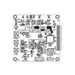
DC1783A-G
Part Number : DC1783A-G
Analog Devices Inc.Data Conversion IC Development Tools LTC2377-18 Demo Board with LTC6655-5/LT6
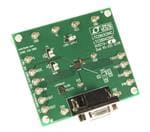
DC827A-A
Part Number : DC827A-A
Analog Devices Inc.Interface Development Tools LTC2803 Demo Board - Dual RS232 Transcei

AD8313ARMZ
Part Number : AD8313ARMZ
Analog Devices Inc.The AD8313 is a complete multistage demodulating logarithmic amplifier that can accurately convert an RF signal at its input to an equivalent decibel-scaled value at its dc output. The AD8313 maintains a high degree of log conformance for signal frequencies from 0.1 GHz to 2.5 GHz. Application is straightforward, requiring only a single supply of 2.7 V to 5.5 V and the addition of a suitable input and supply decoupling. Operating on a 3 V supply, its 13.7 mA consumption (for TA = 25°C) is only 41 mW. A power-down feature is provided; the input is taken high to initiate a low current (20 µA) sleep mode, with a threshold at half the supply voltageThe AD8313 is fabricated on Analog Devices, Inc., advanced 25 GHz silicon bipolar IC process and is available in an 8-lead MSOP package. The operating temperature range is −40°C to +85°C.

AD8402ANZ10
Part Number : AD8402ANZ10
Analog Devices Inc.The AD8400/AD8402/AD8403 provide a single, dual or quad channel, 256 position digitally controlled variable resistor (VR) device. These devices perform the same electronic adjustment function as a potentiometer or variable resistor. The AD8400 contains a single variable resistor in the compact SO-8 package. The AD8402 contains two independent variable resistors in saving SO-14 surface mount package. The AD8403 contains four independent variable resistors in 24-lead PDIP, SOIC and TSSOP packages. Each part contains a fixed resistor with a wiper contact that taps the fixed resistor value at a point determined by a digital code loaded into the controlling serial input register. The resistance between the wiper and either endpoint of the fixed resistor varies linearly with respect to the digital code transferred into the VR latch. Each variable resistor offers a completely programmable value of resistance, between the A terminal and the wiper or the B terminal and the wiper. The fixed A to B terminal resistance of 1 kOhm, 10 kOhm, 50 kOhm or 100 kOhm has a ±1% channel-to-channel matching tolerance with a nominal temperature coefficient of 500 ppm/°C. A unique switching circuit minimizes the high glitch inherent in traditional switched resistor designs avoiding any make-before-break or break-before-make operation.Each VR has its own VR latch that holds its programmed resistance value. These VR latches are updated from an SPI compatible serial-to-parallel shift register that is loaded from a standard 3-wire serial-input digital interface. Ten data bits make up the data word clocked into the serial input register. The data word is decoded where the first two bits determine the address of the VR latch to be loaded, the last eight bits are data. A serial data output pin at the opposite end of the serial register allows simple daisy-chaining in multiple VR applications without additional external decoding logic.
AD8402ARUZ50
Part Number : AD8402ARUZ50
Analog Devices Inc.The AD8400/AD8402/AD8403 provide a single, dual or quad channel, 256 position digitally controlled variable resistor (VR) device. These devices perform the same electronic adjustment function as a potentiometer or variable resistor. The AD8400 contains a single variable resistor in the compact SO-8 package. The AD8402 contains two independent variable resistors in saving SO-14 surface mount package. The AD8403 contains four independent variable resistors in 24-lead PDIP, SOIC and TSSOP packages. Each part contains a fixed resistor with a wiper contact that taps the fixed resistor value at a point determined by a digital code loaded into the controlling serial input register. The resistance between the wiper and either endpoint of the fixed resistor varies linearly with respect to the digital code transferred into the VR latch. Each variable resistor offers a completely programmable value of resistance, between the A terminal and the wiper or the B terminal and the wiper. The fixed A to B terminal resistance of 1 kOhm, 10 kOhm, 50 kOhm or 100 kOhm has a ±1% channel-to-channel matching tolerance with a nominal temperature coefficient of 500 ppm/°C. A unique switching circuit minimizes the high glitch inherent in traditional switched resistor designs avoiding any make-before-break or break-before-make operation.Each VR has its own VR latch that holds its programmed resistance value. These VR latches are updated from an SPI compatible serial-to-parallel shift register that is loaded from a standard 3-wire serial-input digital interface. Ten data bits make up the data word clocked into the serial input register. The data word is decoded where the first two bits determine the address of the VR latch to be loaded, the last eight bits are data. A serial data output pin at the opposite end of the serial register allows simple daisy-chaining in multiple VR applications without additional external decoding logic.

AD8664ARZ
Part Number : AD8664ARZ
Analog Devices Inc.The AD8661 / AD8662 / AD8664 are rail-to-rail output, single-supplyamplifiers that use the Analog Devices, Inc., patentedDigiTrim® trimming technique to achieve low offset voltage.The AD8661 / AD8662 / AD8664 series features extendedoperating ranges, with supply voltages up to 16 V. It alsofeatures low input bias current, wide signal bandwidth,and low input voltage and current noise.The combination of low offset, very low input bias current,and a wide supply range makes these amplifiers useful in a widevariety of applications usually associated with higher priced JFETamplifiers. Systems using high impedance sensors, such asphotodiodes, benefit from the combination of low input biascurrent, low noise, low offset, and wide bandwidth. The wideoperating voltage range meets the demands of high performanceanalog-to-digital converters (ADCs) and digital-to-analogconverters (DACs). Audio applications and medical monitoringequipment can take advantage of the high input impedance, lowvoltage, low current noise, and wide bandwidth.The single AD8661 is available in a narrow 8-lead SOIC packageand a very thin, dual lead, 8-lead LFCSP. The AD8661 SOICpackage is specified over the extended industrial temperaturerange of −40°C to +125°C. The AD8661 LFCSP is specified overthe industrial temperature range of −40°C to +85°C. The AD8662is available in a narrow 8-lead SOIC package and an 8-lead MSOP,both specified over the extended industrial temperature range of−40°C to +125°C. The AD8664 is available in a narrow 14-leadSOIC package and a 14-lead TSSOP, both with an extendedindustrial temperature range of −40°C to +125°C.Applications Sensors Medical equipment Consumer audio Photodiode amplification ADC drivers

AD9763ASTZRL
Part Number : AD9763ASTZRL
Analog Devices Inc.The AD9763/AD9765/AD9767 are dual-port, high speed, 2-channel, 10-/12-/14-bit CMOS DACs. Each part integrates two high quality TxDAC+® cores, a voltage reference, and digital interface circuitry into a small 48-lead LQFP. The AD9763/AD9765/AD9767 offer exceptional ac and dc performance while supporting update rates of up to 125 MSPS.The AD9763/AD9765/AD9767 have been optimized for processing I and Q data in communications applications. The digital interface consists of two double-buffered latches as well as control logic. Separate write inputs allow data to be written to the two DAC ports independent of one another. Separate clocks control the update rate of the DACs.A mode control pin allows the AD9763/AD9765/AD9767 to interface to two separate data ports, or to a single interleaved high speed data port. In interleaving mode, the input data stream is demuxed into its original I and Q data and then latched. The I and Q data is then converted by the two DACs and updated at half the input data rate.The GAINCTRL pin allows two modes for setting the full-scale current (IOUTFS) of the two DACs. IOUTFS for each DAC can be set independently using two external resistors, or IOUTFS for both DACs can be set by using a single external resistor. See the Gain Control Mode section for important date code information on this feature.The DACs utilize a segmented current source architecture combined with a proprietary switching technique to reduce glitch energy and maximize dynamic accuracy. Each DAC provides differential current output, thus supporting single-ended or differential applications. Both DACs of the AD9763, AD9765, or AD9767 can be simultaneously updated and can provide a nominal full-scale current of 20 mA. The full-scale currents between each DAC are matched to within 0.1%.The AD9763/AD9765/AD9767 are manufactured on an advanced, low cost CMOS process. They operate from a single supply of 3.3 V to 5 V and consume 380 mW of power.PRODUCT HIGHLIGHTSThe AD9763/AD9765/AD9767 are members of a pin-compatible family of dual TxDACs providing 8-, 10-, 12-, and 14-bit resolution.Dual 10-/12-/14-Bit, 125 MSPS DACs. A pair of high performance DACs for each part is optimized for low distortion performance and provides flexible transmission of I and Q information.Matching. Gain matching is typically 0.1% of full scale, and offset error is better than 0.02%.Low Power. Complete CMOS dual DAC function operates on 380 mW from a 3.3 V to 5 V single supply. The DAC full-scale current can be reduced for lower power operation, and a sleep mode is provided for low power idle periods.On-Chip Voltage Reference. The AD9763/AD9765/AD9767 each include a 1.20 V temperature-compensated band gap voltage reference.Dual 10-/12-/14-Bit Inputs. The AD9763/AD9765/AD9767 each feature a flexible dual-port interface, allowing dual or interleaved input data.APPLICATIONSCommunicationsBase stationsDigital synthesisQuadrature modulation3D ultrasound

ADE7757ARNZ
Part Number : ADE7757ARNZ
Analog Devices Inc.The ADE7757 is an accurate electrical energy measurement integrated circuit. It is a pin reduction version of ADE7755 with an enhancement of a precise oscillator circuit that serves as a clock source to the chip. The ADE7757 eliminates the cost of an external crystal or resonator, thus reducing the overall cost of a meter built with this IC. The chip directly interfaces with shunt resistor.The ADE7757 provides instantaneous and average real power based on line current and voltage. The part specifications surpass the accuracy requirements as quoted in the IEC61036 standard. The only analog circuitry used in the ADE7757 is in the ADCs and reference circuit. All other signal processing (e.g., multiplication and filtering) is carried out in the digital domain. This approach provides superior stability and accuracy over extremes in environmental conditions and over time.The small analog input full-scale allows the chip to interface to low value shunt resistances without losing dynamic range. The ADE7757 is available in 16-lead SOIC narrow-body package.The Application Note AN-679 can be used as a basis for a description of an IEC61036 low cost, watt-hour meter reference design.NOTE: For polyphase system designs, the ADE7752A is recommended.
ADE7757ARNZRL
Part Number : ADE7757ARNZRL
Analog Devices Inc.The ADE7757 is an accurate electrical energy measurement integrated circuit. It is a pin reduction version of ADE7755 with an enhancement of a precise oscillator circuit that serves as a clock source to the chip. The ADE7757 eliminates the cost of an external crystal or resonator, thus reducing the overall cost of a meter built with this IC. The chip directly interfaces with shunt resistor.The ADE7757 provides instantaneous and average real power based on line current and voltage. The part specifications surpass the accuracy requirements as quoted in the IEC61036 standard. The only analog circuitry used in the ADE7757 is in the ADCs and reference circuit. All other signal processing (e.g., multiplication and filtering) is carried out in the digital domain. This approach provides superior stability and accuracy over extremes in environmental conditions and over time.The small analog input full-scale allows the chip to interface to low value shunt resistances without losing dynamic range. The ADE7757 is available in 16-lead SOIC narrow-body package.The Application Note AN-679 can be used as a basis for a description of an IEC61036 low cost, watt-hour meter reference design.NOTE: For polyphase system designs, the ADE7752A is recommended.


