AD7273BUJZ-500RL7
Part Number : AD7273BUJZ-500RL7
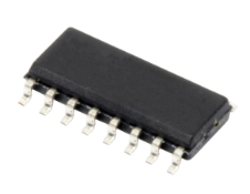
Analog Devices Inc.The AD7273 is a 10-bit, high speed, low power, successive-approximation ADC. The part operates from a single 2.35V to 3.6 V power supply and features throughput rates up to 3 MSPS. The part contains a low-noise, wide bandwidth track/hold amplifier which can handle input frequencies in excess of 30 MHz.The conversion process and data acquisition are controlled using CS and the serial clock, allowing the devices to interface with microprocessors or DSPs. The input signal is sampled on the falling edge of CS and the conversion is also initiated at this point. The conversion rate is determined by the SCLK. There are no pipeline delays associated with the part.The AD7273 uses advanced design techniques to achieve very low power dissipation at high throughput rates.The reference for the part is applied externally and can be in the range of 1.2 V to VDD. This allows the widest dynamic input range to the ADC.PRODUCT HIGHLIGHTS 3 MSPS ADCs in an 8-lead TSOT package. High throughput with low power consumption. Flexible power/serial clock speed management. Allows maximum power efficiency at low throughput rates. Reference can be driven up to the power supply. No pipeline delay. The parts feature a standard successive approximation ADC with accurate control of the sampling instant via a CS input and once-off conversion control.APPLICATIONS Battery-Powered Systems Personal Digital Assistants Medical Instruments Mobile Communications Instrumentation and Control Systems Data Acquisition Systems High-Speed Modems Optical Sensors
AD7641BCPZ
Part Number : AD7641BCPZ
Analog Devices Inc.The AD7641 is a 18-bit, 2 MSPS, charge redistribution SAR, fully differential analog-to-digital converter that operates from a single 2.5 V power supply. The part contains a high-speed 18-bit sampling ADC, an internal conversion clock, an internal reference buffer, error correction circuits, and both serial and parallel system interface ports. It features a very high sampling rate mode (Warp) and a fast mode (Normal) for asynchronous conversion rate applications.The AD7641 is hardware factory calibrated and comprehensively tested to ensure ac parameters such as signal-to-noise ratio (SNR) and total harmonic distortion (THD) in addition to the more traditional dc parameters of gain, offset and linearity. Operation is specified from −40°C to +85°C.PRODUCT HIGHLIGHTS Fast Throughput. The AD7641 is a 2 MSPS, charge redistribution, 18-bit SAR ADC. Superior Linearity. The AD7641 has no missing 18-bit code. Internal Reference. The AD7641 has a 2.048 V internal reference with a typical drift of ±10 ppm/°C and an on-chip TEMP sensor. Single-Supply Operation. The AD7641 operates from a 2.5 V single supply. Serial or Parallel Interface. Versatile parallel (16- or 8-bit bus) or 2-wire serial interface arrangement compatible with 2.5 V, 3.3 V, or 5 V logic.APPLICATIONS Medical instruments High dynamic data acquisition Instrumentation Spectrum analysis ATE
AD7706BRUZ
Part Number : AD7706BRUZ
Analog Devices Inc.The AD7705 / AD7706 are complete analog front ends for low frequency measurement applications. These 2-/3-channel devices can accept low level input signals directly from a transducer and produce serial digital output. The devices employ a Σ-Δ conversion technique to realize up to 16 bits of no missing codes performance. The selected input signal is applied to a proprietary, programmable-gain front end based around an analog modulator. The modulator output is processed by an on-chip digital filter. The first notch of this digital filter can be programmed via an on-chip control register, allowing adjustment of the filter cutoff and output update rate. The AD7705 / AD7706 devices operate from a single 2.7 V to 3.3 V or 4.75 V to 5.25 V supply. The AD7705 features two fully differential analog input channels; the AD7706 features three pseudo differential input channels. Both devices feature a differential reference input. Input signal ranges of 0 mV to 20 mV through 0 V to 2.5 V can be incorporated on both devices when operating with a VDD of 5 V and a reference of 2.5 V. They can also handle bipolar input signal ranges of ±20 mV through ±2.5 V, which are referenced to the AIN(−) inputs on the AD7705 and to the COMMON input on the AD7706.The AD7705 / AD7706 devices, with a 3 V supply and a 1.225 V reference, can handle unipolar input signal ranges of 0 mV to 10 mV through 0 V to 1.225 V. The devices can accept bipolar input ranges of ±10 mV through ±1.225 V. Therefore, the AD7705 / AD7706 devices perform all signal conditioning and conversion for a 2-channel or 3-channel system. The AD7705 / AD7706 are ideal for use in smart, microcontroller, or DSP-based systems. The devices feature a serial interface that can be configured for 3-wire operation. Gain settings, signal polarity, and update rate selection can be configured in software using the input serial port. The parts contains self-calibration and system calibration options to eliminate gain and offset errors on the part itself or in the system. CMOS construction ensures very low power dissipation, and the power-down mode reduces the standby power consumption to 20 μW typ. These parts are available in a 16-lead, wide body (0.3 inch), plastic dual in-line package (DIP); a 16-lead, wide body (0.3 inch), standard small outline (SOIC) package; and a low profile, 16-lead, thin shrink small outline package (TSSOP).
AD7741BNZ
Part Number : AD7741BNZ
Analog Devices Inc.The AD7741/AD7742 are a new generation of synchronous voltage-to-frequency converters (VFCs). The AD7741 is a single-channel version in an 8-lead package (SOIC/DIP) and the AD7742 is a multichannel version in a 16-lead package (SOIC/DIP). No user trimming is required to achieve the specified performance.The AD7741 has a single buffered input whereas the AD7742 has four buffered inputs that may be configured as two fully-differential inputs or three pseudo-differential inputs. Both parts include an on-chip +2.5 V bandgap reference that provides the user with the option of using this internal reference or an external reference.The AD7741 has a single-ended voltage input range from 0 V to REFIN. The AD7742 has a differential voltage input range from –VREF to +VREF. Both parts operate from a single +5 V supply consuming typically 6 mA, and also contain a power down feature that reduces the current consumption to less than 35 μA.Applications Low Cost Analog-to-Digital Conversion Signal Isolation AD7742 is obsolete
AD7796BRUZ-REEL
Part Number : AD7796BRUZ-REEL
Analog Devices Inc.The AD7796/AD7797 are complete, analog front ends for highprecision, bridge sensor applications such as weigh scales. TheAD7796/AD7797 contain a Σ-∆ ADC capable of 16-/24-bitresolution, respectively. The on-chip instrumentation amplifierhas a fixed gain of 128, allowing small amplitude signals such asthose from bridge sensors to be directly interfaced to the ADC.Each device has one differential input and contains a temperaturesensor that is internally connected to the ADC. This sensor canbe used to perform temperature compensation of the bridge.The devices can be operated with the internal clock or an externalclock. The output data rate from the devices is software-programmableand can be varied from 4.17 Hz to 123 Hz.The AD7796/AD7797 operate with a power supply from 2.7 Vto 5.25 V. Each device consumes a current of 250 µA typical andis housed in a 16-lead TSSOP.Applications Weigh scales Strain gages Industrial process control Instrumentation Portable instrumentation
AD7920BKSZ-500RL7
Part Number : AD7920BKSZ-500RL7
Analog Devices Inc.The AD7910 / AD7920 are 10-bit and 12-bit, high speed, low power, successive-approximation ADCs respectively. The parts operate from a single 2.35 V to 5.25 V power supply and feature throughput rates up to 250 kSPS. The parts contain a low-noise, wide bandwidth track/hold amplifier, which can handle input frequencies in excess of 6 MHz.The conversion process and data acquisition are controlled using CS and the serial clock, allowing the devices to interface with microprocessors or DSPs. The input signal is sampled on the falling edge of CS and the conversion is also initiated at this point. There are no pipelined delays associated with the part.The AD7910 / AD7920 use advanced design techniques to achieve very low power dissipation at high throughput rates.The reference for the part is taken internally from VDD. This allows the widest dynamic input range to the ADC. Thus the analog input range for the part is 0 to VDD. The conversion rate is determined by the SCLK.PRODUCT HIGHLIGHTS 10-/12-bit ADCs in SC70 and MSOP packages. Low power consumption. Flexible power/serial clock speed management. The conversion rate is determined by the serial clock, allowing the conversion time to be reduced through the serial clock speed increase. This allows the average power consumption to be reduced when power-down mode is used while not converting. The part also features a power-down mode to maximize power efficiency at lower throughput rates. Current consumption is 1 μA maximum and 50 nA typically when in power-down mode. Reference derived from the power supply. No pipeline delay. The parts feature a standard successive approximation ADC with accurate control of the sampling instant via a CS input and once-off conversion control.APPLICATIONS Battery-powered systems Personal digital assistants Medical instruments Mobile communications Instrumentation and control systems Data acquisition systems High speed modems Optical sensors
AD8027ARZ
Part Number : AD8027ARZ
Analog Devices Inc.The AD8027/AD8028 are high speed amplifiers with rail-to-railinput and output that operate on low supply voltages and areoptimized for high performance and a wide dynamic signal range.The AD8027/AD8028 have low noise (4.3 nV/√Hz, 1.6 pA/√Hz)and low distortion (120 dBc at 1 MHz). In applications that use afraction of or use the entire input dynamic range and requirelow distortion, the AD8027/AD8028 are ideal choices.Many rail-to-rail input amplifiers have an input stage that switchesfrom one differential pair to another as the input signal crossesa threshold voltage, which causes distortion. The AD8027/AD8028have a unique feature that allows the user to select the inputcrossover threshold voltage through the DISABLE/SELECT pin(DISABLE/SELECT x in the 10-lead MSOP, hereafter referredto as DISABLE/SELECT throughout this data sheet). This featurecontrols the voltage at which the complementary transistorinput pairs switch. The AD8027/AD8028 also have intrinsicallylow crossover distortion.With their wide supply voltage range (2.7 V to 12 V) and widebandwidth (190 MHz), the AD8027/AD8028 amplifiers aredesigned to work in a variety of applications where speed andperformance are needed on low supply voltages. The high performanceof the AD8027/AD8028 is achieved with a quiescentcurrent of only 6.5 mA (typical) per amplifier. The AD8027/AD8028 have a shutdown mode that is controlled viathe DISABLE/SELECT pin.The AD8027/AD8028 are available in 8-lead SOIC, 6-lead SOT-23,and 10-lead MSOP packages. The AD8028WARMZ-R7 is anautomotive grade version, qualified for automotive applications.See the Automotive Products section for more details. TheAD8027/AD8028 family is designed to work over the extendedtemperature range of −40°C to +125°C.Applications Filters ADC drivers Level shifting Buffering Professional video Low voltage instrumentation
AD8028ARMZ
Part Number : AD8028ARMZ
Analog Devices Inc.The AD8027/AD8028 are high speed amplifiers with rail-to-railinput and output that operate on low supply voltages and areoptimized for high performance and a wide dynamic signal range.The AD8027/AD8028 have low noise (4.3 nV/√Hz, 1.6 pA/√Hz)and low distortion (120 dBc at 1 MHz). In applications that use afraction of or use the entire input dynamic range and requirelow distortion, the AD8027/AD8028 are ideal choices.Many rail-to-rail input amplifiers have an input stage that switchesfrom one differential pair to another as the input signal crossesa threshold voltage, which causes distortion. The AD8027/AD8028have a unique feature that allows the user to select the inputcrossover threshold voltage through the DISABLE/SELECT pin(DISABLE/SELECT x in the 10-lead MSOP, hereafter referredto as DISABLE/SELECT throughout this data sheet). This featurecontrols the voltage at which the complementary transistorinput pairs switch. The AD8027/AD8028 also have intrinsicallylow crossover distortion.With their wide supply voltage range (2.7 V to 12 V) and widebandwidth (190 MHz), the AD8027/AD8028 amplifiers aredesigned to work in a variety of applications where speed andperformance are needed on low supply voltages. The high performanceof the AD8027/AD8028 is achieved with a quiescentcurrent of only 6.5 mA (typical) per amplifier. The AD8027/AD8028 have a shutdown mode that is controlled viathe DISABLE/SELECT pin.The AD8027/AD8028 are available in 8-lead SOIC, 6-lead SOT-23,and 10-lead MSOP packages. The AD8028WARMZ-R7 is anautomotive grade version, qualified for automotive applications.See the Automotive Products section for more details. TheAD8027/AD8028 family is designed to work over the extendedtemperature range of −40°C to +125°C.Applications Filters ADC drivers Level shifting Buffering Professional video Low voltage instrumentation
AD8313ARMZ
Part Number : AD8313ARMZ
Analog Devices Inc.The AD8313 is a complete multistage demodulating logarithmic amplifier that can accurately convert an RF signal at its input to an equivalent decibel-scaled value at its dc output. The AD8313 maintains a high degree of log conformance for signal frequencies from 0.1 GHz to 2.5 GHz. Application is straightforward, requiring only a single supply of 2.7 V to 5.5 V and the addition of a suitable input and supply decoupling. Operating on a 3 V supply, its 13.7 mA consumption (for TA = 25°C) is only 41 mW. A power-down feature is provided; the input is taken high to initiate a low current (20 µA) sleep mode, with a threshold at half the supply voltageThe AD8313 is fabricated on Analog Devices, Inc., advanced 25 GHz silicon bipolar IC process and is available in an 8-lead MSOP package. The operating temperature range is −40°C to +85°C.
AD8402ANZ10
Part Number : AD8402ANZ10
Analog Devices Inc.The AD8400/AD8402/AD8403 provide a single, dual or quad channel, 256 position digitally controlled variable resistor (VR) device. These devices perform the same electronic adjustment function as a potentiometer or variable resistor. The AD8400 contains a single variable resistor in the compact SO-8 package. The AD8402 contains two independent variable resistors in saving SO-14 surface mount package. The AD8403 contains four independent variable resistors in 24-lead PDIP, SOIC and TSSOP packages. Each part contains a fixed resistor with a wiper contact that taps the fixed resistor value at a point determined by a digital code loaded into the controlling serial input register. The resistance between the wiper and either endpoint of the fixed resistor varies linearly with respect to the digital code transferred into the VR latch. Each variable resistor offers a completely programmable value of resistance, between the A terminal and the wiper or the B terminal and the wiper. The fixed A to B terminal resistance of 1 kOhm, 10 kOhm, 50 kOhm or 100 kOhm has a ±1% channel-to-channel matching tolerance with a nominal temperature coefficient of 500 ppm/°C. A unique switching circuit minimizes the high glitch inherent in traditional switched resistor designs avoiding any make-before-break or break-before-make operation.Each VR has its own VR latch that holds its programmed resistance value. These VR latches are updated from an SPI compatible serial-to-parallel shift register that is loaded from a standard 3-wire serial-input digital interface. Ten data bits make up the data word clocked into the serial input register. The data word is decoded where the first two bits determine the address of the VR latch to be loaded, the last eight bits are data. A serial data output pin at the opposite end of the serial register allows simple daisy-chaining in multiple VR applications without additional external decoding logic.
AD8402ARUZ50
Part Number : AD8402ARUZ50
Analog Devices Inc.The AD8400/AD8402/AD8403 provide a single, dual or quad channel, 256 position digitally controlled variable resistor (VR) device. These devices perform the same electronic adjustment function as a potentiometer or variable resistor. The AD8400 contains a single variable resistor in the compact SO-8 package. The AD8402 contains two independent variable resistors in saving SO-14 surface mount package. The AD8403 contains four independent variable resistors in 24-lead PDIP, SOIC and TSSOP packages. Each part contains a fixed resistor with a wiper contact that taps the fixed resistor value at a point determined by a digital code loaded into the controlling serial input register. The resistance between the wiper and either endpoint of the fixed resistor varies linearly with respect to the digital code transferred into the VR latch. Each variable resistor offers a completely programmable value of resistance, between the A terminal and the wiper or the B terminal and the wiper. The fixed A to B terminal resistance of 1 kOhm, 10 kOhm, 50 kOhm or 100 kOhm has a ±1% channel-to-channel matching tolerance with a nominal temperature coefficient of 500 ppm/°C. A unique switching circuit minimizes the high glitch inherent in traditional switched resistor designs avoiding any make-before-break or break-before-make operation.Each VR has its own VR latch that holds its programmed resistance value. These VR latches are updated from an SPI compatible serial-to-parallel shift register that is loaded from a standard 3-wire serial-input digital interface. Ten data bits make up the data word clocked into the serial input register. The data word is decoded where the first two bits determine the address of the VR latch to be loaded, the last eight bits are data. A serial data output pin at the opposite end of the serial register allows simple daisy-chaining in multiple VR applications without additional external decoding logic.
AD8664ARZ
Part Number : AD8664ARZ
Analog Devices Inc.The AD8661 / AD8662 / AD8664 are rail-to-rail output, single-supplyamplifiers that use the Analog Devices, Inc., patentedDigiTrim® trimming technique to achieve low offset voltage.The AD8661 / AD8662 / AD8664 series features extendedoperating ranges, with supply voltages up to 16 V. It alsofeatures low input bias current, wide signal bandwidth,and low input voltage and current noise.The combination of low offset, very low input bias current,and a wide supply range makes these amplifiers useful in a widevariety of applications usually associated with higher priced JFETamplifiers. Systems using high impedance sensors, such asphotodiodes, benefit from the combination of low input biascurrent, low noise, low offset, and wide bandwidth. The wideoperating voltage range meets the demands of high performanceanalog-to-digital converters (ADCs) and digital-to-analogconverters (DACs). Audio applications and medical monitoringequipment can take advantage of the high input impedance, lowvoltage, low current noise, and wide bandwidth.The single AD8661 is available in a narrow 8-lead SOIC packageand a very thin, dual lead, 8-lead LFCSP. The AD8661 SOICpackage is specified over the extended industrial temperaturerange of −40°C to +125°C. The AD8661 LFCSP is specified overthe industrial temperature range of −40°C to +85°C. The AD8662is available in a narrow 8-lead SOIC package and an 8-lead MSOP,both specified over the extended industrial temperature range of−40°C to +125°C. The AD8664 is available in a narrow 14-leadSOIC package and a 14-lead TSSOP, both with an extendedindustrial temperature range of −40°C to +125°C.Applications Sensors Medical equipment Consumer audio Photodiode amplification ADC drivers
AD9763ASTZRL
Part Number : AD9763ASTZRL
Analog Devices Inc.The AD9763/AD9765/AD9767 are dual-port, high speed, 2-channel, 10-/12-/14-bit CMOS DACs. Each part integrates two high quality TxDAC+® cores, a voltage reference, and digital interface circuitry into a small 48-lead LQFP. The AD9763/AD9765/AD9767 offer exceptional ac and dc performance while supporting update rates of up to 125 MSPS.The AD9763/AD9765/AD9767 have been optimized for processing I and Q data in communications applications. The digital interface consists of two double-buffered latches as well as control logic. Separate write inputs allow data to be written to the two DAC ports independent of one another. Separate clocks control the update rate of the DACs.A mode control pin allows the AD9763/AD9765/AD9767 to interface to two separate data ports, or to a single interleaved high speed data port. In interleaving mode, the input data stream is demuxed into its original I and Q data and then latched. The I and Q data is then converted by the two DACs and updated at half the input data rate.The GAINCTRL pin allows two modes for setting the full-scale current (IOUTFS) of the two DACs. IOUTFS for each DAC can be set independently using two external resistors, or IOUTFS for both DACs can be set by using a single external resistor. See the Gain Control Mode section for important date code information on this feature.The DACs utilize a segmented current source architecture combined with a proprietary switching technique to reduce glitch energy and maximize dynamic accuracy. Each DAC provides differential current output, thus supporting single-ended or differential applications. Both DACs of the AD9763, AD9765, or AD9767 can be simultaneously updated and can provide a nominal full-scale current of 20 mA. The full-scale currents between each DAC are matched to within 0.1%.The AD9763/AD9765/AD9767 are manufactured on an advanced, low cost CMOS process. They operate from a single supply of 3.3 V to 5 V and consume 380 mW of power.PRODUCT HIGHLIGHTSThe AD9763/AD9765/AD9767 are members of a pin-compatible family of dual TxDACs providing 8-, 10-, 12-, and 14-bit resolution.Dual 10-/12-/14-Bit, 125 MSPS DACs. A pair of high performance DACs for each part is optimized for low distortion performance and provides flexible transmission of I and Q information.Matching. Gain matching is typically 0.1% of full scale, and offset error is better than 0.02%.Low Power. Complete CMOS dual DAC function operates on 380 mW from a 3.3 V to 5 V single supply. The DAC full-scale current can be reduced for lower power operation, and a sleep mode is provided for low power idle periods.On-Chip Voltage Reference. The AD9763/AD9765/AD9767 each include a 1.20 V temperature-compensated band gap voltage reference.Dual 10-/12-/14-Bit Inputs. The AD9763/AD9765/AD9767 each feature a flexible dual-port interface, allowing dual or interleaved input data.APPLICATIONSCommunicationsBase stationsDigital synthesisQuadrature modulation3D ultrasound
ADE7757ARNZRL
Part Number : ADE7757ARNZRL
Analog Devices Inc.The ADE7757 is an accurate electrical energy measurement integrated circuit. It is a pin reduction version of ADE7755 with an enhancement of a precise oscillator circuit that serves as a clock source to the chip. The ADE7757 eliminates the cost of an external crystal or resonator, thus reducing the overall cost of a meter built with this IC. The chip directly interfaces with shunt resistor.The ADE7757 provides instantaneous and average real power based on line current and voltage. The part specifications surpass the accuracy requirements as quoted in the IEC61036 standard. The only analog circuitry used in the ADE7757 is in the ADCs and reference circuit. All other signal processing (e.g., multiplication and filtering) is carried out in the digital domain. This approach provides superior stability and accuracy over extremes in environmental conditions and over time.The small analog input full-scale allows the chip to interface to low value shunt resistances without losing dynamic range. The ADE7757 is available in 16-lead SOIC narrow-body package.The Application Note AN-679 can be used as a basis for a description of an IEC61036 low cost, watt-hour meter reference design.NOTE: For polyphase system designs, the ADE7752A is recommended.
AD8599ARZ-REEL
Part Number : AD8599ARZ-REEL
Analog Devices Inc.The AD8597/AD8599 are very low noise, low distortion opera-tional amplifiers ideal for use as preamplifiers. The low noise of 1.1 nV/√Hz and low harmonic distortion of −120 dB (or better) at audio bandwidths give the AD8597/AD8599 the wide dynamic range necessary for preamplifiers in audio, medical, and instru-mentation applications. The excellent slew rate of 14 V/μs and 10 MHz gain bandwidth make them highly suitable for medical applications. The low distortion and fast settling time make them ideal for buffering of high resolution data converters.The AD8597 is available in 8-lead SOIC and LFCSP packages, while the AD8599 is available in an 8-lead SOIC package. They are both specified over a −40°C to +125°C temperature range. The AD8597 and AD8599 are members of a growing series of low noise op amps offered by Analog Devices, Inc.Applications Professional audio preamplifiers ATE/precision testers Imaging systems Medical/physiological measurements Precision detectors/instruments Precision data conversion
AD8605ARTZ-REEL7
Part Number : AD8605ARTZ-REEL7
Analog Devices Inc.The AD8605, AD8606, and AD8608 are single, dual, and quad rail-to-rail input and output, single-supply amplifiers. They feature very low offset voltage, low input voltage and current noise, and wide signal bandwidth. They use the Analog Devices, Inc. patented DigiTrim® trimming technique, which achieves superior precision without laser trimming.The combination of low offsets, low noise, very low input bias currents, and high speed makes these amplifiers useful in a wide variety of applications. Filters, integrators, photodiode amplifiers, and high impedance sensors all benefit from the combination of performance features. Audio and other ac applications benefit from the wide bandwidth and low distortion. Applications for these amplifiers include optical control loops, portable and loop-powered instrumentation, and audio amplification for portable devices.The AD8605, AD8606, and AD8608 are specified over the extended industrial temperature range (−40°C to +125°C). The AD8605 single is available in 5-lead SOT-23 and 5-ball WLCSP packages. The AD8606 dual is available in an 8-lead MSOP, an 8-ball WLSCP, and a narrow SOIC surface-mounted package. The AD8608 quad is available in a 14-lead TSSOP package and a narrow 14-lead SOIC package. The 5-ball and 8-ball WLCSP offer the smallest available footprint for any surface-mounted operational amplifier. The WLCSP, SOT-23, MSOP, and TSSOP versions are available in tape-and-reel only.Applications Photodiode amplification Battery-powered instrumentation Multipole filters Sensors Barcode scanners Audio
AD8606ARZ-REEL
Part Number : AD8606ARZ-REEL
Analog Devices Inc.The AD8605, AD8606, and AD8608 are single, dual, and quad rail-to-rail input and output, single-supply amplifiers. They feature very low offset voltage, low input voltage and current noise, and wide signal bandwidth. They use the Analog Devices, Inc. patented DigiTrim® trimming technique, which achieves superior precision without laser trimming.The combination of low offsets, low noise, very low input bias currents, and high speed makes these amplifiers useful in a wide variety of applications. Filters, integrators, photodiode amplifiers, and high impedance sensors all benefit from the combination of performance features. Audio and other ac applications benefit from the wide bandwidth and low distortion. Applications for these amplifiers include optical control loops, portable and loop-powered instrumentation, and audio amplification for portable devices.The AD8605, AD8606, and AD8608 are specified over the extended industrial temperature range (−40°C to +125°C). The AD8605 single is available in 5-lead SOT-23 and 5-ball WLCSP packages. The AD8606 dual is available in an 8-lead MSOP, an 8-ball WLSCP, and a narrow SOIC surface-mounted package. The AD8608 quad is available in a 14-lead TSSOP package and a narrow 14-lead SOIC package. The 5-ball and 8-ball WLCSP offer the smallest available footprint for any surface-mounted operational amplifier. The WLCSP, SOT-23, MSOP, and TSSOP versions are available in tape-and-reel only.Applications Photodiode amplification Battery-powered instrumentation Multipole filters Sensors Barcode scanners Audio
AD8608ARUZ-REEL
Part Number : AD8608ARUZ-REEL
Analog Devices Inc.The AD8605, AD8606, and AD8608 are single, dual, and quad rail-to-rail input and output, single-supply amplifiers. They feature very low offset voltage, low input voltage and current noise, and wide signal bandwidth. They use the Analog Devices, Inc. patented DigiTrim® trimming technique, which achieves superior precision without laser trimming.The combination of low offsets, low noise, very low input bias currents, and high speed makes these amplifiers useful in a wide variety of applications. Filters, integrators, photodiode amplifiers, and high impedance sensors all benefit from the combination of performance features. Audio and other ac applications benefit from the wide bandwidth and low distortion. Applications for these amplifiers include optical control loops, portable and loop-powered instrumentation, and audio amplification for portable devices.The AD8605, AD8606, and AD8608 are specified over the extended industrial temperature range (−40°C to +125°C). The AD8605 single is available in 5-lead SOT-23 and 5-ball WLCSP packages. The AD8606 dual is available in an 8-lead MSOP, an 8-ball WLSCP, and a narrow SOIC surface-mounted package. The AD8608 quad is available in a 14-lead TSSOP package and a narrow 14-lead SOIC package. The 5-ball and 8-ball WLCSP offer the smallest available footprint for any surface-mounted operational amplifier. The WLCSP, SOT-23, MSOP, and TSSOP versions are available in tape-and-reel only.Applications Photodiode amplification Battery-powered instrumentation Multipole filters Sensors Barcode scanners Audio
AD9203WARUZ
Part Number : AD9203WARUZ
Analog Devices Inc.The AD9203 is a monolithic low power, single supply, 10-bit, 40 MSPS analog-to-digital converter with an on-chip voltage reference. It uses a multistage differential pipeline architecture at 40 MSPS data rate and guarantees no missing codes over the full operating temperature range. Its input range may be adjusted between 1 V and 2 VP-P.The ADC has an on-board programmable reference. An external reference can also be chosen to suit the DC accuracy and temperature drift requirements of an application. An external resistor can be used to reduce power consumption when operating at lower sampling rates.A single clock input is used to control all internal conversion cycles. The digital output data is presented in straight binary or two's complement output format. An out-of-range signal (OTR) indicates an over-flow condition that can be used with the most significant bit to determine over-flow or under-flow. The AD9203 can operate with a supply range from 2.7 V to 3.6 V, attractive for low power operation in high-speed portable applications.Fabricated on an advanced CMOS process, the AD9203 is available in a 28-pin thin shrink small outline package (28 TSSOP) specified over the industrial temperature range (−40°C to +85°C).
AD9211BCPZ-250
Part Number : AD9211BCPZ-250
Analog Devices Inc.The AD9211 is a 10-bit monolithic sampling analog-to-digital converter optimized for high performance, low power, and ease of use. The product operates at up to a 300 MSPS conversion rate and is optimized for outstanding dynamic performance in wideband carrier and broadband systems. All necessary functions, including a track-and-hold (T/H) and voltage reference, are included on the chip to provide a complete signal conversion solution.The ADC requires a 1.8 V analog voltage supply and a differential clock for full performance operation. The digital outputs are LVDS (ANSI-644) compatible and support either twos complement, offset binary format, or Gray code. A data clock output is available for proper output data timing.Fabricated on an advanced CMOS process, the AD9211 is available in a 56-lead LFCSP, specified over the industrial temperature range (−40°C to +85°C).PRODUCT HIGHLIGHTS High Performance—Maintains 60.1 dBFS SNR @ 300 MSPS with a 70 MHz input. Low Power—Consumes only 410 mW @ 300 MSPS. Ease of Use—LVDS output data and output clock signal allow interface to current FPGA technology. The on-chip reference and sample-and-hold provide flexibility in system design. Use of a single 1.8 V supply simplifies system power supply design. Serial Port Control—Standard serial port interface supports various product functions, such as data formatting, disabling the clock duty cycle stabilizer, power-down, gain adjust, and output test pattern generation. Pin-Compatible Family—12-bit pin-compatible family offered as AD9230.APPLICATIONS Wireless and wired broadband communications Cable reverse path Communications test equipment Radar and satellite subsystems Power amplifier linearization


