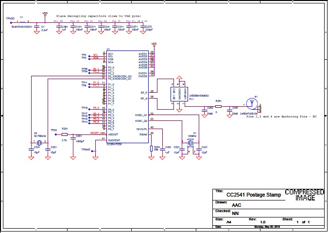
CC2541 Postage Stamp Reference Design
Description
The CC2541 Postage Stamp reference design contains the schematics and layout files for the CC2541PS Module. The reference design demonstrates good techniques for CC2541 decoupling and RF layout for a very compact 16.3mm x 13mm PCB . For optimum RF performance: the reference design should be copied accurately. This is a 2-layer PCB reference design using an integrated solution of a Johanson Chip balun(2450BM15A0002) and a Johanson chip antenna(2450AT42A100). The CC2541 Postage stamp is perfect for applications requiring proximity detecting and temperature sensing. It is ideal for proof of concept prototyping on existing systems.
Features
- Affordable low cost: 2 layer board design in a compact form factor of 16.3mmX13mm Onboard chip antenna (from Johanson: 2450AT42A100) with integrated balun (from Johanson: 2450BM15A002) matching circuit: with 1 SPI: 1 I2C and 1 USART interface pinout Can be used for proximity sensing: temp data logging: quick prototyping and quick PoC (Proof of Concept) purposes Free schematics: BOM and gerber available online for download
Applications
Product Categories
- Low-power 2.4-GHz products
| Title | Updated | Type | Size (KB) |
|---|---|---|---|
| AN081 -- Johanson Technology Balun Optimized for CC253X, CC254X, CC257X, CC853X (Rev. B) | 06 Nov 2012 | 456 | |
| AN098 - Layout Review Techniques for Low Power RF Designs (Rev. A) | 02 Aug 2012 | 456 | |
| AN058 -- Antenna Selection Guide (Rev. B) | 06 Oct 2010 | 1836 |
| Download | |
|---|---|
| Download the bill of materials for CC2541-POSTAGE-STAMP-RD | Download |
Schematic

Quickly understand overall system functionality.
Download the schematic for CC2541-POSTAGE-STAMP-RD| Title | Updated | Type | Size (KB) | |
|---|---|---|---|---|
| CC2541 Postage Stamp Reference Design Bill of Materials (BOM) (Rev. A) | 14 Oct 2013 | 97 | ||
| CC2541 Postage Stamp Reference Design Schematic (Rev. A) | 14 Oct 2013 | 25 | ||
| CC2541 Postage Stamp Reference Design Assembly Drawing (Rev. A) | 14 Oct 2013 | 27 |